Analysis and Improvement of Quality Defects in PCB Inner Layers (Coating Process)
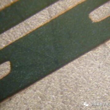
1. PCB Inner Layer Defects – Open Circuits, Notches, Pinholes 1. Common Defects (Open Circuits, Notches, Pinholes) Image Description 1.1. Open Circuit due to Ink Peeling (caused by poor surface treatment affecting ink adhesion) 1.2. Notch in the Circuit (Pinholes on the Ink Surface after Coating) 1.3. Open Circuit (Debris on the Film Positioning) 1.4. … Read more