Abstract
This article introduces how Advanced Micro Devices (AMD) customizes laser detection solutions based on reconfigurable FPGA devices, replacing traditional instrument configurations. By utilizing the flexible and customizable FPGA device Moku, it provides more efficient and adaptable laser detection technology. The article discusses multiple case studies that explore how the Moku platform simplifies experimental setups, deploys phase-locked amplifiers and dual boxcar averagers to enhance signal quality, and optimizes real-time signal processing through Moku’s neural network and cloud compilation capabilities. Moku integrates various functions such as signal generation, test analysis, and control adjustments into a single device, supporting users in quickly deploying custom HDL code. This solution features high integration, low hardware investment costs, simple configuration, and supports highly customizable and advanced signal processing technologies.
01
Introduction
Currently, the integration of laser probe (LP) technology and its derived applications heavily relies on solutions provided by original equipment manufacturers (OEMs). However, these comprehensive solutions generally lack flexibility and generalizability, and often face restrictions related to intellectual property. The legal and financial processes required for coordination with suppliers are usually complex and time-consuming, which greatly hinders the progress of technological innovation in actual production and affects research collaboration among scientific institutions in this field.FPGA (Field Programmable Gate Array) is an integrated circuit that can be programmed and reconfigured by users, suitable for high-speed parallel processing and real-time data processing applications. Modern FPGAs typically integrate hardware and software IP cores, enhancing their functionality and supporting applications such as embedded processors, RF signal processing, and AI acceleration. The partial reconfiguration capability of FPGAs allows users to build low-latency, customized test configurations, simplifying wiring and reducing signal loss. Additionally, FPGAs support dynamic hot-swapping, allowing functionalities to be added or removed without interfering with other instruments.
HaoLiang Optoelectronics代理的Liquid Instruments的Moku设备 is a high-performance test and measurement platform developed based on FPGA technology, integrating up to 15 types of specialized test and measurement instrument functions, such as oscilloscopes, phase-locked amplifiers, signal generators, etc. It employs advanced ADC hybrid technology, significantly improving the device’s baseline noise performance, ensuring more accurate measurement results, especially with excellent low-frequency noise performance. Moku supports multi-instrument parallel operation, capable of running up to eight instruments simultaneously, with high synchronization between instruments on the clock bus, reducing additional noise and improving experimental efficiency. This highly integrated design greatly simplifies experimental configurations, reduces hardware connection complexity, and enhances the reliability of signal processing. Furthermore, Moku’s cloud compilation feature allows users to customize instrument functions and testing processes according to specific needs, flexibly addressing various challenges in real-time data processing, waveform generation, and signal analysis. By defining instruments through software, Moku provides an easy-to-operate, precise, flexible, and customizable solution for laser probe technology.
In this article, we will showcase multiple case studies demonstrating the reconfigurable integrated solutions based on Moku and their improvements compared to traditional methods. First, we will introduce two alternative implementations of frequency domain mapping, using a single Moku to replace the complex setup of multiple instruments in traditional solutions: one is using Moku’s phase-locked amplifier, which can directly switch between the local oscillator and the phase-locked loop, outputting high signal-to-noise ratio signals, reducing the scanning area and increasing scanning speed; the other is using Moku’s Python API and cloud compilation feature to deploy a dual boxcar averager in real-time, easily capturing all signal components within the gated window under more complex background noise. Next, we will explore how to implement this method using the dual boxcar averager. After that, we will provide a customized solution based on Moku’s phase-locked amplifier to improve signal quality. Finally, we will investigate artificial intelligence, particularly through the neural network (NN) functionality provided by Moku, to improve the application of laser probe signal acquisition in real-time signal processing.The solutions presented in this article are compatible with any commercial laser scanning microscope (LSM) equipped with low-noise lasers and appropriate bandwidth detectors. As shown in Figure 1, most commercial LSMs provide at least one photon detector output, which can transmit the electrical signal of the device under test (DUT) reflecting the electrical excitation; one analog auxiliary input for converting the signal into grayscale image pixels; and one external synchronization input for synchronizing the laser system.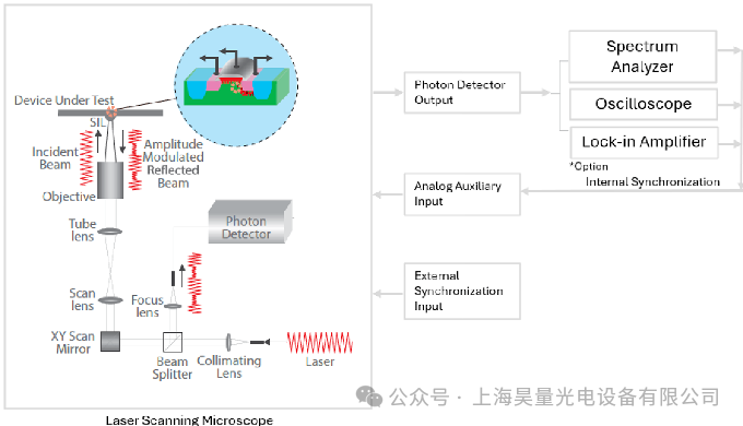 Figure 1: External input/output interfaces of commercial laser scanning microscopes, using the default laser detection and frequency domain mapping configuration.The low-frequency and mid-frequency configurations provided by LSM manufacturers typically require the use of standalone instruments such as oscilloscopes and spectrum analyzers to achieve corresponding technologies. For instance, the implementation of time domain mapping requires a phase-locked amplifier with boxcar averaging functionality, which is usually offered as an additional option. The reconfigurable integrated solution based on Moku greatly simplifies this setup, requiring only one reconfigurable FPGA device, Moku, and two physical connections: one connected to the photon detector output and the other connected to the analog auxiliary input, as shown in Figure 2. In this configuration, due to the limitations of the LSM software, laser synchronization will not be used. Once the hardware connections are established, these instruments can be completely switched through the software interface. Next, we will discuss in more detail how to implement a customizable laser detection solution through Moku.
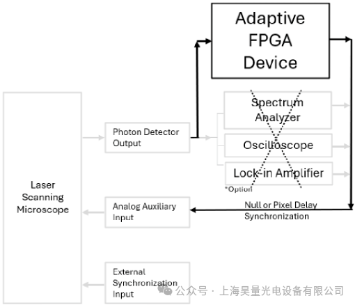 Figure 2: Simplified implementation of laser detection technology compared to the default configuration of the original equipment manufacturer (with some parts crossed out). Deploying a single reconfigurable FPGA device Moku can replace all three independent measuring instruments (spectrum analyzer, oscilloscope, and phase-locked amplifier).
02
Frequency Domain Mapping Solution
Frequency domain mapping is typically used to align laser images with mold layouts and ensure precise focusing, which is crucial for achieving optimal signal acquisition.First, we implement frequency domain mapping using the software-defined phase-locked amplifier deployed on the reconfigurable FPGA device Moku. This phase-locked amplifier provides a phase-locked loop (PLL) that can generate sine waves precisely aligned with DUT synchronization pulse signals. As shown in Figure 3, if phase information is needed, the DUT synchronization pulse can be directly connected to Moku; otherwise, using the internal oscillator is sufficient. The specific configuration requires setting the desired experimental frequency in the internal oscillator or PLL module and selecting either rectangular or polar coordinate output, depending on whether phase information is needed or if only amplitude demodulation frequency domain mapping is required, as shown in Figure 4. The final output is a frequency domain mapping signal with a high signal-to-noise ratio (SNR), supporting fast scanning and reducing the scanning area.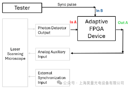 Figure 3: Physical hardware connection between the reconfigurable FPGA device and LSM
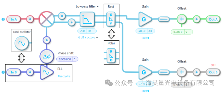 Figure 4: Configuration of Moku’s phase-locked amplifier for frequency mapping technology. It can switch between the local oscillator and the phase-locked loop to output amplitude or phase information.Therefore, by observing real-time frequency domain mapping scanning results, the optical focus can be adjusted in real-time to achieve optimal optical focusing effects. Figure 5 (upper part) shows the continuous frequency domain mapping images captured during the focusing operation. To achieve the best focusing effect, both P-type and N-type active regions must exhibit their global maximum contrast values. In Figure 5 (lower part), a contrast map drawn from the dashed rectangular area in the upper part of Figure 5 is provided. This map quantitatively depicts the contrast changes of the P-type and N-type active regions. Image number 4 meets the criteria for optimal focusing, as it shows both P-type and N-type active regions with globally maximum contrast. This statistical method has potential application value in future automated processes.
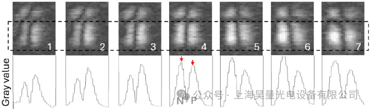 Figure 5: Sequence of frequency domain mapping images during the focal length adjustment process. Image number 4 has the best focusing effect.
It should be noted that the frequency domain mapping performance is optimal when the target frequency is periodic (e.g., clock signals or HHLL-based flattened scanning signals) and has a duty cycle of approximately 50%. Deviations from a 50% duty cycle introduce additional harmonics, negatively impacting system performance and reducing overall signal-to-noise ratio.
Additionally, using the software-defined dual boxcar averager (Moku provides a Python API control panel and cloud compilation deployment to achieve this functionality) can also implement frequency domain mapping. In the time domain, the baseline boxcar is set at the zero voltage level of the clock signal, while the pulse boxcar is set at the effective clock position, as shown in Figure 6. Depending on the length of the test mode, frequency, and allowable laser power, the dual boxcar averager can achieve a good signal-to-noise ratio with over 2000 averages and can achieve faster scanning rates. Figure 7 compares the results obtained from different frequency domain mapping implementations. Overall, compared to the phase-locked amplifier method, when the background signal is more complex, as shown in Figure 8, it captures all signal components within the gated window, while the phase-locked amplifier method only captures signal components at the target frequency. Users can choose the appropriate frequency domain mapping method based on their specific objectives.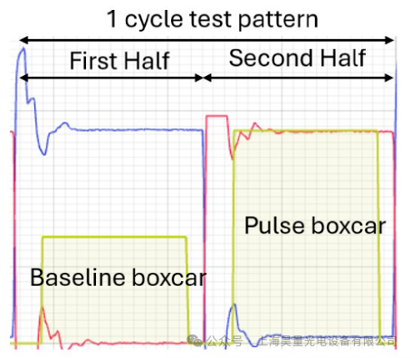 Figure 6: The blue line represents the displayed waveform without clock signal vectors. The red line represents the displayed waveform with valid clock signal vectors. The yellow shaded areas are the baseline boxcar (lower) and pulse boxcar (higher).
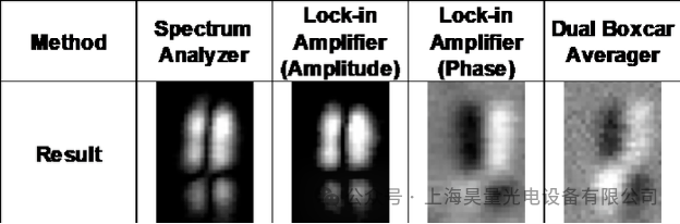 Figure 7: Comparison of different frequency domain mapping implementations
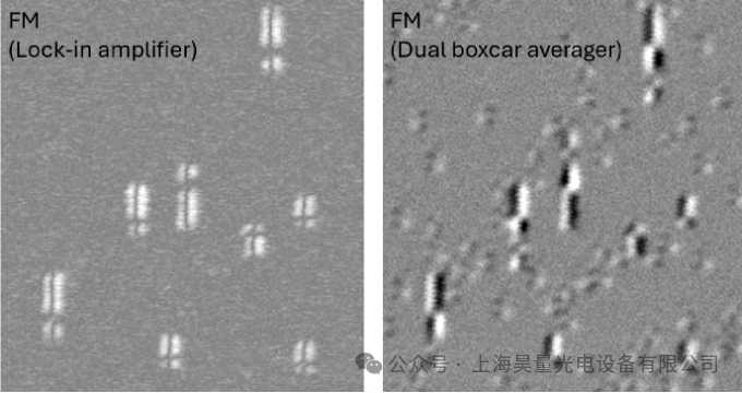 Figure 8: The frequency domain mapping results obtained using the dual boxcar averager are often richer than those obtained using the phase-locked amplifier.
03
Time Domain Mapping Solution
When implementing the time domain mapping solution using the reconfigurable FPGA device Moku, no changes are needed to the hardware connections shown in Figure 3; simply switch the deployed software-defined instrument from the phase-locked amplifier to the dual boxcar averager module. Configure the pulse boxcar to capture the desired signal position and the baseline boxcar at the position without a signal. Finally, align the laser pixel delay with the boxcar averaging time, as shown in Figure 9.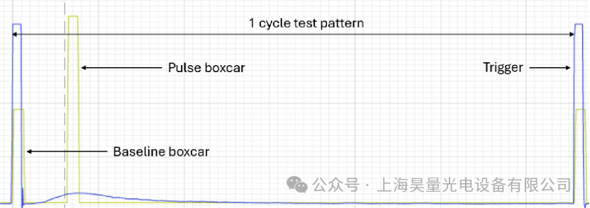 Figure 9: Example of the time waveform for time domain mapping. The trigger signal (blue) is provided by the test device. The baseline boxcar (lower yellow line) is set at the position without a signal, while the pulse boxcar (higher yellow line) is set at the position where the signal needs to be captured.Time domain mapping is particularly effective in tracking non-periodic signals or low duty cycle periodic signals (e.g., signals generated by compressed scanning modes) in the transistor’s time domain dynamic characteristics. Figure 10 shows the application of time domain modulation to the scanning unit under test, where the input buffer is at SI and the output buffer is at SO. The missing time domain mapping signal is detected starting from the output part of the scanning unit and extends to output buffer B. Further examination using laser detection reveals that the output of the scanning unit does not flip with the excitation signal.
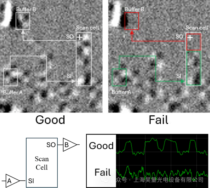 Figure 10: Time domain mapping result images displayed on normal and faulty components. Compared to normal components, the time domain mapping signal on faulty components is missing from the scanning unit output area to output buffer B. The laser detection signal of the faulty component is marked with a ‘+’ at the scanning unit output, indicating that it exhibits output behavior that does not flip with the excitation signal.Time domain mapping also demonstrates significant value in precise probe positioning, providing a faster alternative to the time-consuming traditional multi-point acquisition method, and alleviating issues when the probing laser wavelength does not match the imaging laser wavelength. However, the processing speed of time domain mapping is inherently slower, requiring at least three orders of magnitude of averaging cycles. Typically, time domain mapping is performed using a reduced scanning window, and it is recommended to optimize the length of the test pattern for maximum efficiency.
04
Custom Solution Example—Moving Average Filter
Next, we will specifically demonstrate how to meet specific measurement needs by deploying a custom solution on Moku. Specifically, we simultaneously deployed a phase-locked amplifier and a custom real-time moving average filter in Moku’s multi-instrument parallel mode, allowing them to work together to achieve a simple frequency domain mapping solution.In multi-instrument parallel mode, users can deploy up to 8 instruments to run simultaneously, flexibly configuring the required instruments based on experimental needs, with instruments highly synchronized on the clock bus.As shown in Figure 11, the custom algorithm required for this implementation is deployed through the cloud compilation module. The data interaction and synchronization between the two instruments used in this solution are configured through the internal interconnect structure of the FPGA, ensuring low-latency signal transmission without any additional physical wiring between instruments.
The implementation principle of the moving average filter is given by the following formula
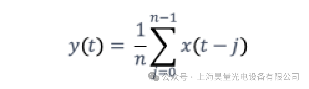 where x(t) is the discrete time series input signal, y(t) is the output signal, and n is the number of samples of the continuous signal. This equation is implemented through HDL code and compiled into a bitstream file, which can then be deployed via the cloud compiler.
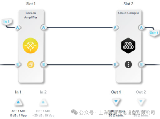
Figure 11: Series configuration of Moku’s multi-instrument parallel mode. The output A of the phase-locked amplifier is connected to the input A of the cloud compiler, which deploys the custom algorithm of the moving average filter.
This filter has a low computational load, requiring only an accumulator, a subtractor, and a shift operation. Therefore, it has very low latency, making it very suitable for real-time applications. As shown in the actual measurement results in Figure 12, the measured delay between the input and output of the moving average filter implemented in the example is 224 nanoseconds, equivalent to 70 clock cycles of a 312.5 MHz FPGA clock.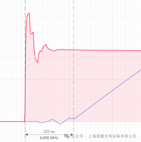 Under a 50 MHz FPGA system clock, the delay between the input and output of the phase-locked amplifier and the moving average filter is approximately 222 nanoseconds. The red line represents the input, and the blue line represents the output of the moving average filter.This moving average filter can reduce the noise amplitude to the square root of the original value multiplied by 2 raised to the power of n. In our implementation, n = 8, so the noise amplitude should be reduced to 1/16, which corresponds to the signal amplitude increasing to 16 times its original value. In the results shown in Figure 13, the output and input of the moving average filter are measured at 360 mV and 22 mV, respectively, approximately 16.4 times, which meets theoretical expectations. With the higher signal-to-noise ratio provided by the moving average filter, laser power can be reduced, or faster scanning speeds can be achieved by reducing pixel dwell time while maintaining comparable output results.
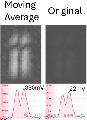 Figure 13: Comparison of output after adding the moving average filter with the original output of the phase-locked amplifier; output voltages are 360 mV and 22 mV, respectively.
05
Implementation of Noise Reduction Solution Based on Neural Networks
The reconfigurable and parallel processing architecture of FPGAs is very suitable for neural network processing. It provides low-latency inference performance, suitable for various real-time signal processing applications such as signal denoising, classification, and closed-loop control. Next, we will use neural networks such as autoencoders for signal denoising and deploy them through Moku for front-end signal processing before inputting to other instruments (such as oscilloscopes, phase-locked amplifiers, and boxcar averagers). An autoencoder is a type of neural network designed to efficiently learn compressed representations of input data. It accomplishes this by adopting a network architecture that compresses the data into a smaller encoded space representation and then reconstructs it back to the original input size.
5.1 Autoencoder
Before inputting a series of time series data into the neural network, it is converted into a format of 32 parallel data using a sliding window containing 32 data points. As shown in Figure 14, we configured a four-layer autoencoder. The sizes of the encoding spaces for the first three layers are set to 16-2-16, with each layer using the Tanh function, while the last layer uses a linear function, aggregating the decoded data into a single output. This autoencoder is trained using randomly generated white noise data with a mean of zero and a normal distribution.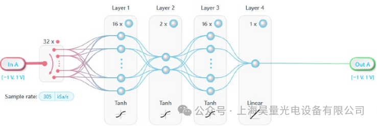 Figure 14: A four-layer autoencoder structure based on a time data sliding window.Considering the current allocation of FPGA resources, the input sampling rate of the neural network is set at 305 kSa/s; however, our test setup and the bandwidth of the laser probe detector are incompatible, somewhat limiting our further exploration. Nevertheless, we conducted a series of software simulation tests to study the behavior of the autoencoder neural network. We added normally distributed random white noise to a square wave with an amplitude of ±0.5 V.
5.2 Performance Evaluation
To evaluate the noise suppression performance, we adopted the standard deviation difference (SDD) as an indicator, which measures the standard deviation of the difference between the processed signal and the true value, rather than using mean square error (MSE). Compared to MSE, SDD more consistently reflects the denoising results relative to the true value in various scenarios. As shown in Figure 15, the performance of the autoencoder given by MS differs from that of the median filter by more than 8 times (8.9975 vs 0.9347). In contrast, SDD can more accurately reflect actual performance, showing that the SDD of the median filter is lower (the lower, the better) than that of the autoencoder (0.1551 vs 0.3814).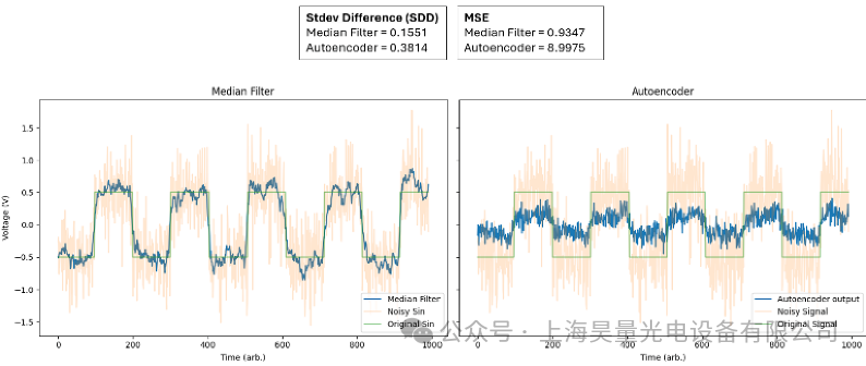 Figure 15: Comparison of median filter and autoencoder in terms of SDD and MSE evaluation metrics.
5.3 Offset Compensation
In the output results of the autoencoder, a negative offset of 5 data points is observed compared to the true value, as shown in Figure 16. This offset is only significantly visible in the simulation environment, as no delay processing is considered in the simulation. In practical applications, this negative offset is usually negligible, as the instrument’s delay would be significantly longer, and real data for direct comparison cannot be obtained. In this case study, we always compensated for the 5 data point offset.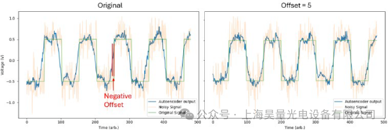 Figure 16: The original output of the autoencoder with negative offset and the compensated version.
5.4 Sampling
To test the performance of the autoencoder at different sampling rates or data densities, we defined the sampling rate as the number of samples collected per signal pulse. In laser detection applications, the sampling rate is typically set to collect between 50 to 200 samples per signal pulse to achieve reliable resolution for analysis, with specific values depending on the frequency of the test setup and the performance of the oscilloscope. The results shown in Figure 17 indicate that the performance of the autoencoder improves as data density increases, but begins to stabilize when reaching 400 samples/pulse.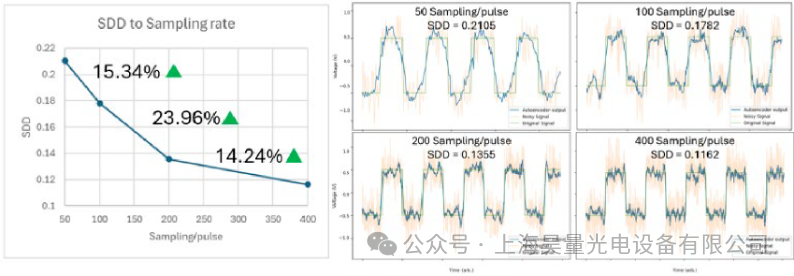 Figure 17: Performance of the autoencoder at different sampling rates. The lower the sampling rate, the smaller the SDD value, the better the performance.
5.5 Noise Levels
We also conducted simulation tests on the autoencoder under different input noise levels. The noise was defined and generated based on random normal distribution at different standard deviations. The results in Figure 18 indicate that the autoencoder performs better under low noise conditions, while its performance begins to decline sharply as noise levels increase.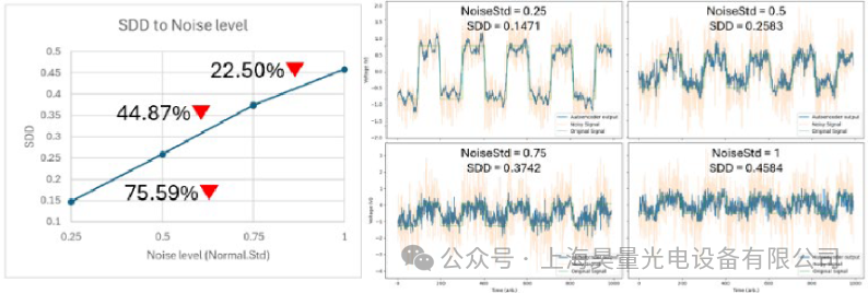 Figure 18: Performance of the autoencoder under different noise levels. *The lower the SDD, the better.
5.6 Number of Neural Network Layers
For the autoencoder structure, we tested different numbers of neural network layers and encoding space sizes. The results indicate that the autoencoder performs better when the encoding space is compressed to the minimum allowable size (i.e., 2). As the number of neural network layers increases from 3 to 5, performance also improves, but when the number of layers increases from 5 to 7, performance declines.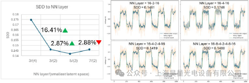 Figure 19: Performance of the autoencoder under different numbers of neural network layers and encoding space sizes. *The lower the SDD, the better.
5.7 Solution Comparison
In a high noise input environment, we conducted comparative tests between the autoencoder and the median filter, using normally distributed data with a mean of 0 and a standard deviation of 2. The test results indicate that the median filter significantly outperforms the average filter (in noise input scenarios) and the autoencoder.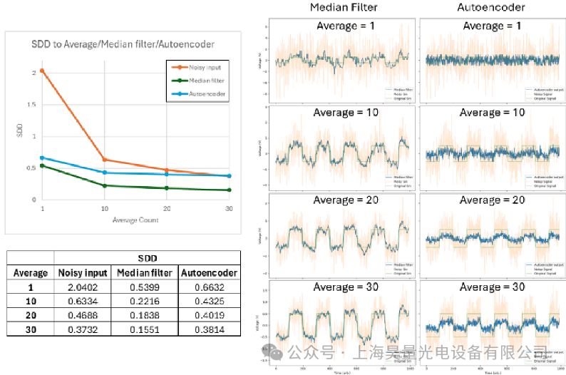 Figure 20: Comparison of performance between autoencoder, mean filter, and median filter.
5.8 Experimental Summary
The above experiments indicate that the autoencoder performs well under high data density and low noise levels. However, when the standard deviation of the input normal distribution noise exceeds 0.25, the autoencoder is no longer suitable as a front-end signal denoising solution. In such cases, the median filter combined with averaging processing will be more appropriate, as it can adapt to a wider range of input data densities and noise levels. Future research can focus on other training datasets or feedback neural network structures—such as recurrent neural networks.
Conclusion
Here, we would like to express our special thanks to AMD engineer Zhi Hao Ko for providing application research and support. This article demonstrates a simple implementation solution for laser detection technology based on a single adaptive FPGA device, validated through practical application cases. The functionality of this FPGA platform is not limited to reconfigurable test and measurement instruments but can also serve as a highly customizable signal processing solution, meeting diverse and specific testing needs and promoting innovation in the testing and measurement field.
The application implementation presented in this article is only a preliminary exploration. In the future, this solution can not only be expanded to more complex optical fault localization technologies but also provide new ideas and implementation paths for a broader range of failure analysis and testing methods. The concept of real-time neural networks (Live NN) still holds great potential in the field of signal processing. As the Moku platform adopts higher-performance FPGA architectures, the system can further enhance sampling and processing capabilities. Additionally, various neural network models can be explored in the future to achieve better performance in terms of accuracy and response speed.
About Moku
Moku is a multifunctional test and measurement platform developed by HaoLiang Optoelectronics代理的Liquid Instruments based on FPGA technology, combining high-bandwidth analog-to-digital converters and digital-to-analog converters to achieve various instrument functions such as signal generation, control adjustments, and test analysis. With its innovative software-defined precision measurement technology, Moku integrates 15 different test and measurement instrument functions into a single device, including phase-locked amplifiers, laser frequency controllers, high-precision phase meters, time interval analyzers, machine learning neural networks, oscilloscopes, and arbitrary waveform generators. Users can flexibly combine these instrument functions according to application needs, enabling simultaneous operation and building customized test and measurement systems. Furthermore, Moku’s cloud compilation feature supports user programming, further enhancing its adaptability and scalability in various scientific research and engineering applications. The latest high-performance model Moku:Delta not only continues the flexibility of Moku’s software-defined instruments but also comprehensively upgrades software and hardware performance:
-
8 analog input and 8 analog output channels, with bandwidth up to 2 GHz
-
14-bit and 20-bit ADC hybrid patented technology, achieving low baseline noise measurements while ensuring high resolution
-
Excellent phase noise and long-term stability
-
Supports Verilog, HDL, and IP core deployment of custom algorithms to FPGA, enabling custom test systems
-
Multi-instrument parallel mode upgraded to support 8 instruments running simultaneously
References
Zhi Hao Ko, Amitesh Kumar, Jobin Thomas Valliyakalayil; November 16–20, 2025. “Laser Probe Techniques with Adaptive FPGA Device.” Proceedings of the ISTFA 2025. ISTFA 2025: Conference Proceedings from the 51st International Symposium for Testing and Failure Analysis. Pasadena, California, USA. (pp. pp. 129-135). ASM.
Contact Us>>>
If you wish to apply for a trial of Moku or discuss your applications with us, please contact us via phone, email, or WeChat.

Regional Manager for the North, Mr. Xu

Regional Manager for the South, Mr. Wang
Related Recommendations
Power Device Dynamic Parameter Testing System Based on Moku: A Precise, Efficient, and Economical Integrated Testing Solution
Moku:Delta Open Prototype Trial! Accelerating the Testing and Verification Process of Semiconductor Devices
Newly Upgraded MokuOS 4.0, Simplifying Cross-Device Platform Collaboration
Moku:Lab Applied to Reconfigurable Integrated Photonic Circuits Based on Organic Nano-Stepping Optical Actuators
“Precise Quantum Bit Control and Readout” White Paper
Moku:Go Affordable Phase-Locked Amplifier is Here!
Max Planck Institute for Polymer Research Uses Moku:Pro to Achieve NV Center-Based Magnetic Field Measurement
AI Intelligent Reconfigurable Testing and Measurement Platform, Moku:Delta Integrates the Industry’s First “Generative Instrument”
Reconfigurable Testing Smart Upgrade | The New Generation Intelligent Control Platform Moku:Delta Released!
New Product Launch | Moku:Delta Debuts
Moku Integrated Quantum Measurement and Control: Software-Defined Instruments Empowering Quantum Sensing and Quantum Metrology
Using Moku Time Interval and Frequency Analyzer to Measure the Micromotions of Trapped Ions
Moku Achieves Single Photon Pair Coincidence Counting Experiment Guidelines
Phase-Locked Amplifier for Research on Dual-Channel and Multi-Instrument Mode SRS Microscopy of Biological Samples