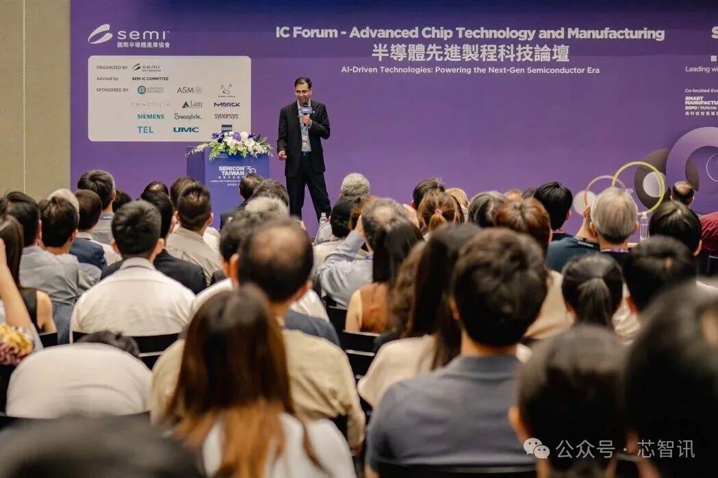
On September 16, according to Taiwan’s “Economic Daily News,” Applied Materials, a leading semiconductor equipment manufacturer, showcased key technologies in advanced packaging, process innovation, and sustainability at the “SEMICON Taiwan 2025” international semiconductor exhibition forum, emphasizing how these technological advancements empower the future of AI. The extensive and interconnected materials engineering solutions from Applied Materials can address the most complex technical challenges in the semiconductor industry and facilitate significant device transformations that form the foundation of AI and high-performance computing.
Yü Dinglu, Vice President of Applied Materials and President of Taiwan Region, pointed out, “Applied Materials is transforming rapid innovation into real impact. Our unique integrated materials engineering solutions help customers improve yield, accelerate time-to-market, promote sustainability, and enhance chip performance. By enabling next-generation chip innovations, Applied Materials is injecting momentum into the AI era and reshaping the future of computing technology.”
To tackle the most complex technical challenges in the semiconductor industry and build the next generation of AI chips, Applied Materials proposed four major solutions:
First, as AI chips scale to 20 trillion transistors, far exceeding the limits of current process technologies, challenges such as stitching, alignment, and stacking errors arise in chip miniaturization processes. Applied Materials has introduced a maskless, GPU-driven “Digital Lithography Technology” (DLT), which features critical dimension uniformity of less than 2 microns and overlay accuracy of less than 0.5 microns, effectively overcoming these bottlenecks to achieve large-scale heterogeneous integration of next-generation AI chips.
Second, for 2-nanometer and more advanced logic components and material innovations, Applied Materials provides breakthrough materials and process innovations to meet the AI-driven semiconductor demands. Its advanced technologies enable next-generation logic architectures, including Gate-All-Around (GAA) transistors, backside power delivery, and stacked Complementary Field Effect Transistors (CFET). With industry-leading solutions in hard mask patterning, low-resistance metallization, and precision planarization and measurement, Applied Materials assists chip manufacturers in enhancing performance and yield in 2-nanometer and more advanced processes. At the forum, Applied Materials also introduced a comprehensive optimization framework for materials, components, circuits, and systems, aimed at significantly improving the performance of various chips, including AI accelerators.
Third, as the industry shifts from system-on-chip to system-in-package, advanced packaging is transforming semiconductor manufacturing by integrating front-end and back-end processes, enhancing efficiency, scalability, and computational power for high-performance computing and edge applications. Applied Materials drives heterogeneous integration processes through key technologies such as hybrid bonding, silicon vias, fan-out, bumps, silicon photonics, and rectangular substrate 3D stacking technologies to accelerate innovation and drive the future development of AI and advanced computing.
Finally, in assisting the semiconductor manufacturing industry to achieve net-zero carbon emissions, Applied Materials addresses the decarbonization challenges of the semiconductor industry through its 2040 net-zero strategy. Applied Materials emphasizes that the company adopts a quantitative, system-level strategy focused on providing solutions and services that reduce wafer fab energy consumption and carbon emissions without compromising operational efficiency. These initiatives aim to promote scalable sustainable development across operations and the value chain, demonstrating Applied Materials’ commitment to supporting global climate action in the semiconductor industry.
Editor: Lin Zi, Chip Intelligence
Previous Exciting ArticlesNVIDIA Violates Antitrust Laws, Facing a Fine of 9.8 Billion Yuan!Arm Executive Responds to Xiaomi’s Self-Developed Chips!Regarding Chips, the Ministry of Commerce Takes Action! Two Major Associations Respond!Micron DRAM Expected to Pause Pricing, Anticipated to Increase by 30%!Domestic Substitution Accelerates! China Launches Anti-Dumping Investigation Against US Analog Chips!Oracle Reportedly Lays Off in China: Compensation N+6!Breaking! The US Adds 23 Chinese Entities Including Fudan Micro to the “Entity List”Zhaoxin KX-7000 Empowers Seewo PC, Aiding Digital Transformation in EducationWei Shaojun: China Should Abandon Using NVIDIA GPUs for AI DevelopmentArm Lumex CSS Released: Detailed Explanation of the New C1 CPU and G1-Ultra GPUPerformance Below Expectations, Synopsys Lays Off 10%! Stock Price Plummets 35%Apple iPhone 17 Series Released: Featuring Three Self-Developed Chips!ASICs Criticized, Broadcom Refutes, NVIDIA Claims Its GPUs Offer Better Value!Dell China Conducts Major Layoffs, Compensation N+3!Hu Yuhua Appointed Senior Vice President of Sales and Marketing for NXP Greater ChinaAMD: No Advantage of Arm Architecture Compared to x86!
For industry communication and collaboration, please add WeChat: icsmart01Chip Intelligence Official Group: 221807116