Follow and StarEmbedded Inn, Exciting News Delivered Promptly[Introduction] Hello everyone, I am Yijun. In the previous article, I summarized the industrial HART bus. Today, let’s talk about the RS-485 bus. RS-485 is also a widely used communication interface. This article will discuss the key points; it is a bit long, about 5000 words.
History and Evolution
RS-485, what does RS mean? It stands for Recommended Standard, and 485 is the standard identification number. As for why this identification number was set, there is no need to delve into it. RS-485 is also known as ANSI/TIA/EIA-485. These prefixes are abbreviations of standard associations’ names, such as EIA, which stands for the Electronics Industries Association. In 1983, the RS-485 communication interface was approved by the Electronics Industries Association as a communication interface standard.Even in today’s booming IoT era, RS-485 still has a large number of applications. Many protocols use RS-485 as the physical layer. For example, which commonly used standard protocols use RS-485 as the physical layer? For instance:
Industrial HART Bus
Modbus Protocol
Profibus DP
…….
Electrical Characteristics
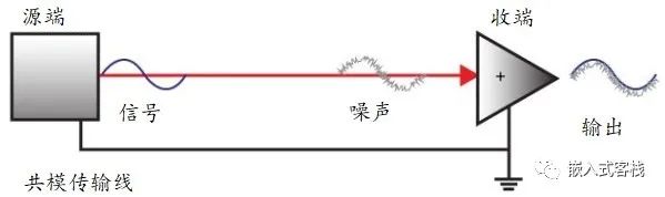
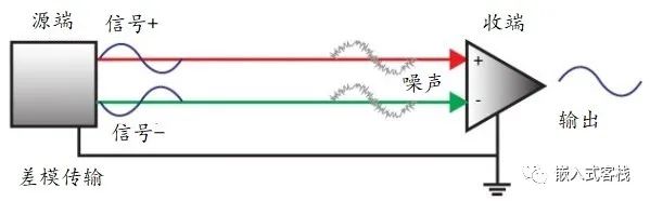
Signal sampling is done through differential transmission, where differential refers to the context of common mode. Differential is also known as differential mode. So what kind of transmission is differential? A picture is worth a thousand words; just look at the two diagrams below:
Common Mode Transmission
When using common mode transmission, common mode noise will superimpose on the final output signal, polluting the original signal.
Differential Mode Transmission
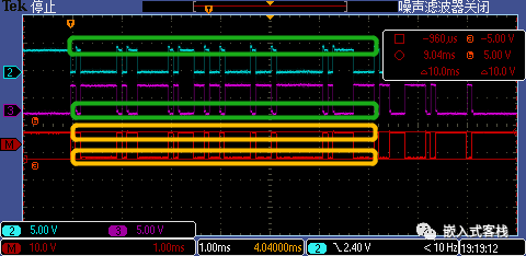
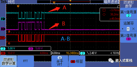
In contrast, when using differential mode transmission, the signals + and – emitted from the source have opposite phases. For common mode noise, it exists on both lines; ideally, they should have equal amplitude and same phase. The receiving end acts like a subtractor, where the useful signal remains due to opposite phases, while the noise gets canceled out. In actual circuits, however, the noise is significantly reduced.Thus, it can be seen that differential transmission has the advantage of effectively canceling common mode interference compared to common mode transmission.Differential mode is sometimes referred to as balanced mode, while common mode is also known as unbalanced mode.To illustrate this interference, let’s take a look at a waveform:At the edges of the A/B signals, the waveforms are slightly distorted, but when you look at A-B (red is the oscilloscope’s MATH subtraction function for A-B), the edges become very clean! This example illustrates that differential transmission can effectively resist common mode interference.
Electrical Parameters
The electrical parameters of RS-485 are:
Common mode voltage range: -7 to +12V
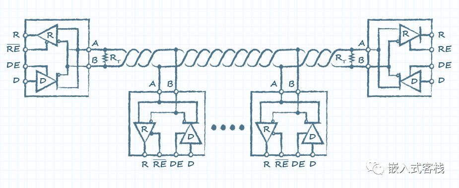
Supports up to 32 multipoint topologies; see the network topology diagram below
When using a 40-foot cable, transmission rates can reach 10Mbps; 1 foot is equivalent to 30.48cm, and Mbps stands for megabits per second
When using a 4000-foot cable, transmission rates can reach 100kbps
Half-duplex communication
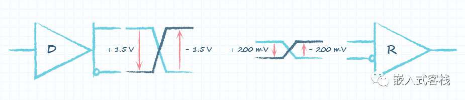
Minimum differential voltage tolerance: 200mV, meaning that if the differential voltage at the receiving end is below 200mV, it cannot correctly identify 0/1. How should this be understood?
How should the above diagram be understood? The RS-485 transceiver’s sending circuit must provide at least 1.5V differential voltage output capability. Due to bus line impedance attenuation, 32 receiver circuit input impedances, and 120Ω termination resistors, the differential signal amplitude will inevitably diminish. Therefore, at the very end, at least 200mV differential voltage must be provided to the terminal receiving circuit.
: The receiving circuit determines the difference between the common mode voltages of line A and line B:
If , the receiving circuit R recognizes it as logic 1
If , the receiving circuit R recognizes it as logic 0
In simple terms, if the absolute voltage value of line A is at least 200mV greater than that of line B, it is recognized as logic 1; or if the absolute voltage value of line A is at least 200mV less than that of line B, it is recognized as logic 0
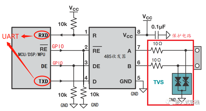
The parameters here should be theoretical values under certain characteristic impedance cables. In actual engineering applications, adjustments and field testing are necessary. Generally, it is best not to exceed these theoretical limits.Speaking of electrical characteristic parameters, let’s first look at a typical interface circuit:From this interface circuit, there are several key points:
RS-485 communication from a microcontroller/DSP/processor interface uses the UART interface with the RS-485 transceiver interface. Of course, you might ask if I can use FPGA; the answer is yes, you can implement a UART transceiver IP module with FPGA. You could even say that using GPIO to simulate UART is also possible, but it’s not very meaningful as it requires CPU resources to implement the low-level bit transmission.
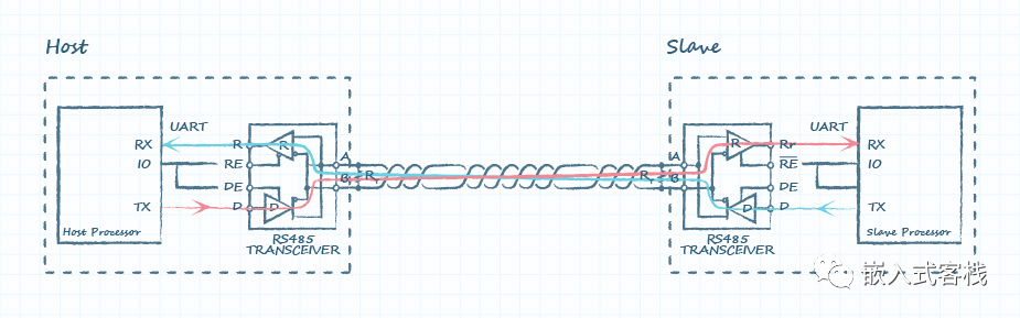
As mentioned earlier, half-duplex implies that there is full-duplex. What is half-duplex? First, half-duplex and full-duplex must be defined in a point-to-point context. Here, point-to-point means at the same time, where half-duplex means that a device is either in the data receiving state or in the data transmitting state at the same time, but cannot do both simultaneously.
Full-duplex, on the other hand, allows for simultaneous sending and receiving. For example, I2C is a half-duplex bus, a 4-wire SPI is full-duplex, while a 3-wire SPI is a half-duplex bus; RS-422 or RS-232 are full-duplex interfaces; CAN bus is half-duplex. RS-485 is a half-duplex bus:
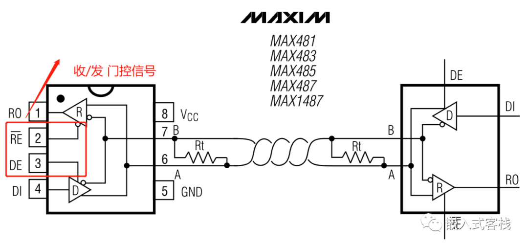
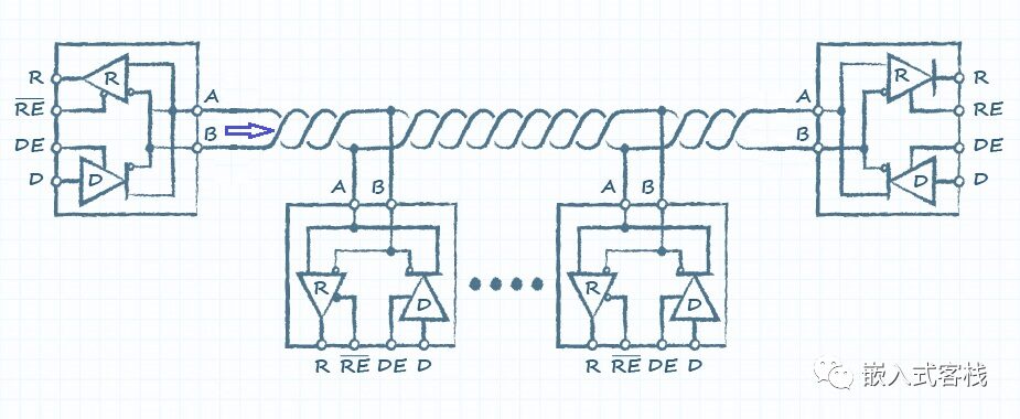
When the Host sends data, the data travels along the red line through the twisted pair to the Slave’s differential receiving circuit. When the Slave responds, the data travels along the blue direction back to the Host’s receiving circuit. However, since the transmission medium is a pair of twisted wires, one side cannot transmit signals while the other is transmitting data. From the transceiver control perspective:A GPIO pin is used to control the receive/transmit enable, and a schematic diagram of the internal principle of the chip makes it easy to understand:
When DIR=0, the receiving circuit is enabled, and the sending circuit is disabled (DE=0), which is equivalent to high impedance for the bus; when DIR=1, the receiving circuit is enabled, and the sending circuit is disabled (DE=1), and the A/B signals depend on the DI signal. Here are two questions:1. Why does the chip design the as opposite effective logic? This is actually convenient for controlling the send/receive circuit with one GPIO.2. Why doesn’t the transceiver chip have a single pin for send/receive enable? For example, why not just call it DIR? It could be made into two separate pins for send/receive control, for instance, :
It is even possible to set DE=1 to 0, allowing for self-looping. Such designs can be implemented in products to achieve self-diagnosis of the transceiver and wiring by comparing the received messages with the sent messages. This can diagnose issues such as chip soldering, transceiver damage, or wiring short circuits.However, you might say this is contradictory! Earlier, you said RS-485 cannot transmit and receive simultaneously, but here you say it can; isn’t that contradictory? It’s not contradictory. What was mentioned earlier about not being able to transmit and receive simultaneously refers to not being able to receive messages sent by other devices while transmitting. Here, the received messages are the ones sent by itself.
Therefore, the essence of half-duplex is that the communication medium does not have a bidirectional channel. When sending data to the bus, the medium is occupied, and even if you want to send, it cannot correctly transmit the signal to the medium. If forced to send, the data will become disordered, and the transceiver chip may even get damaged.
: Receiver Output Enable, enabling the receiver,
DE: Driver Output Enable, enabling the driver output
The DIR pin in the diagram controls whether the RS-485 is in “receive” or “transmit” mode.
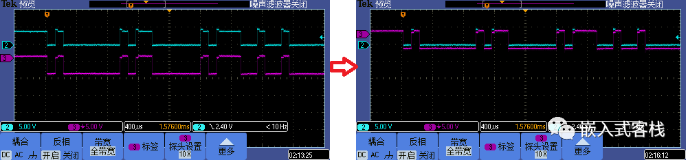
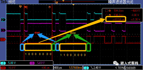
Earlier, we discussed common mode voltage indicators and differential transmission methods; let’s take a look at the waveforms:Channel CH2 connects to the 485 output A, and channel CH3 connects to the 485 output B. The red line represents the oscilloscope’s MATH function: CH2-CH3. Most oscilloscopes have mathematical functions.If you want to view the differential signal, you can use a dual-channel oscilloscope with the MATH subtraction function. If your oscilloscope lacks the MATH function, you can use a trick:Invert the negative terminal of channel B (the differential signal) and align it to the idle level; this way, you can intuitively observe A-B.From this diagram, what valuable signal characteristics can we discover?
Signal A is high when idle; signal B is low when idle. Thus, you will see devices labeled as 485_A+ and 485_B-.
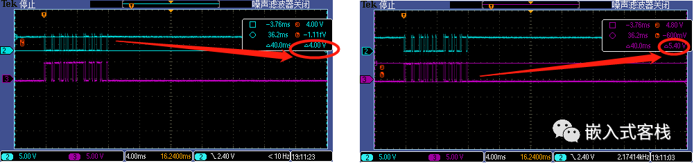
Each channel’s common mode voltage is within the standard requirement of -7 to 12V. Signal A is 4V, and signal B is 5V:
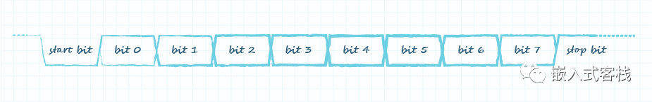
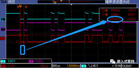
So how do we interpret the data?The captured data is a MODBUS-RTU master sending a message to the slave device. The first two bytes are 0x01 0x03; in UART mode, there is 1 start bit, 8 data bits, 1 stop bit, no parity bit, and the low byte comes first. In this example, the UART communication format is:First, calculate several parameters based on the UART communication mode, including bit time and byte time:This diagram shows that the start bit width is exactly 104us.For analyzing asynchronous serial timing waveforms, the most important aspect is to calculate bit time and byte time based on the communication format, which can then directly parse the waveform data. From this perspective, if you want to implement a UART protocol logic analyzer using FPGA, this is the core metric. By detecting the start bit edge, you can parse the data along the timeline. Here, I will act as a visual UART logic analyzer:The 8-bit data’s time width is exactly 832us. Since the format is low byte first, it needs to be viewed in reverse, which matches the actual sent data of 0x01 0x03.When debugging the lower level, if issues arise, this method can be used to check whether the software correctly drives the hardware. For instance, similar checks can be conducted for I2C/SPI and other lower-level interfaces by examining hardware waveforms. The only difference is that I2C/SPI are synchronous communications, meaning their communication layer has a synchronization clock signal; I2C’s SCL and SPI’s SCK are synchronous clocks.
Driving Capability
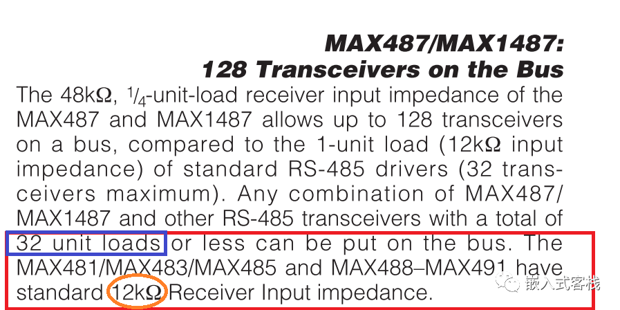
The electrical parameters summarize that RS-485’s maximum electrical driving capability can drive up to 32 stations in a multipoint network topology. How should this indicator be interpreted?First, let’s examine the characteristics of a station’s transmitting and receiving circuit. The standard equivalent input impedance of the receiver circuit of the transceiver is 12kΩ; for example, take the MAX 485 data sheet as a reference:Why 32? This is primarily due to the 200mV minimum driving capability requirement.You can also understand that each receiver circuit’s input impedance is not ideally high, but rather 12kΩ. For instance, if one station sends, it is equivalent to having 32 stations’ input impedances in parallel. Why 32? Don’t forget that the sending station itself also has a receiving circuit. Thus, without considering termination resistors and line impedance, an equivalent load is connected to the sending circuit, and the sending circuit’s driving capability is limited, making it easier to understand.The following diagram illustrates what is called a multipoint network topology, where all stations are arranged along the twisted pair and connected to the bus.Thus, you may see the term “unit load” in some places referring to an RS-485 load, where a unit load refers to a 12kΩ standard input impedance, which is defined by the EIA-485 standard. Hence, terms like unit load originate from this.
Data Monitoring
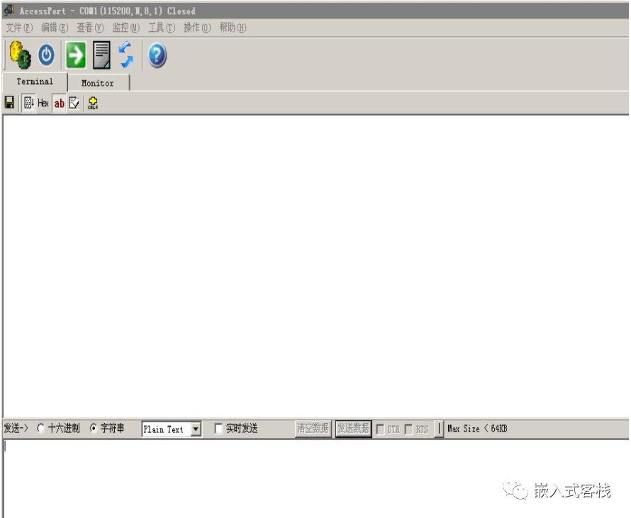
For example, in an RS-485-based Modbus-RTU multipoint network, when programming protocols or debugging multi-station buses, you may need to monitor all messages on the bus. It may even be necessary to implement a bus message recorder to log all messages on the bus. How should this be achieved?Buy a USB to RS-485 converter cable or make one yourself. Connect the A/B lines to the bus, plug the USB into the computer, and use a serial monitoring terminal or write a small serial reception software to monitor all messages on the bus.For instance, the AccessPort serial tool is quite useful:
Application Design
In application design, consider the following dimensions:
Termination Design
Interface Chip
Isolation Design
Termination Design
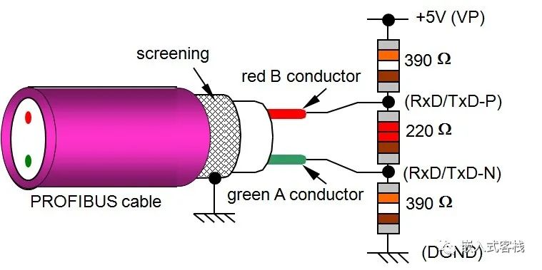
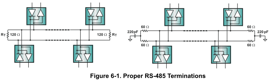
First, why is termination necessary? This is because RS-485 uses twisted pair transmission, and the standard specifies that the characteristic impedance of twisted pairs is between 100Ω and 150Ω. The RS-485 standard developers chose 120Ω as the nominal characteristic impedance.Assuming the signal is sent from the left station, if there is no termination, the signal will experience continuous impedance along the transmission line. However, upon reaching the right side, the equivalent impedance becomes the input impedance of the receiving circuit, such as 12kΩ, leading to a discontinuity in impedance! Some of the signal energy will reflect back along the original path, and the reflected signal will interfere with the original signal due to reactance and inductance, causing errors in communication. In severe cases, communication may not proceed correctly.To gain a deeper understanding of the underlying principles, you can study transmission line theory.Those who have worked with Profibus DP (which also uses RS-485 at the physical layer) may wonder why the recommended termination circuit for Profibus DP is as shown below:This is because the communication medium used by Profibus DP has a different nominal characteristic impedance. Therefore, there may be slight differences in actual engineering applications.In TI’s documentation, there is a termination method illustrated:In noisy environments, it is recommended to use the termination scheme on the right, utilizing two 60Ω resistors and a 220pF capacitor to form a low-pass filter, enhancing the line’s noise immunity.In practical engineering wiring, if encountering severe noise, one can use an oscilloscope to check the bus signal quality and make minor adjustments to the termination method.
Interface Design
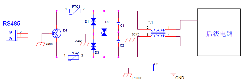
Many chip manufacturers, such as TI and Microchip, provide RS-485 transceiver chips. When selecting an interface chip, consider whether the chip’s power supply voltage input logic is compatible with the levels of the microcontroller/DSP being used. Additionally, check whether the receiver circuit’s impedance complies with the RS-485 standard input impedance. If it does not, adjustments may be necessary in the network deployment regarding the number of loads it can carry. Also, note that some new designs of RS-485 transceivers have fail-safe features.Moreover, as mentioned earlier, standard transceivers can drive up to 32 standard load devices, which is equivalent to (12kΩ) standard unit input impedance.When designing specific interface circuits, also consider EMC requirements. In some environments, there can be significant interference, such as large inductive devices running on the power grid. These can sometimes interfere with devices; there may also be spatial radiation interference. In such cases, consider using shielded twisted pairs with the shield grounded. My knowledge of interference protection is not very deep, but I will summarize it here. I found a lightning protection interface circuit design that can serve as a reference:https://www.programmersought.com/article/95833359295/Earlier, it was mentioned that standard RS-485 can accommodate 32 standard receiver impedance devices. In actual systems, if you want to connect more than 32 station devices, what should you do? You can design a relay device. This is akin to connecting two network segments using a relay to address insufficient driving capability. There are also ready-made products available for this purpose.
Isolation Design
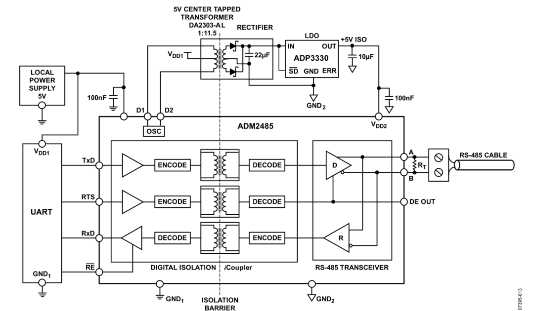
Why is isolation necessary? To reduce ground noise. In many sites, there may be large current switching devices, inductive devices, etc., and noise may couple into the device through the communication ground. Especially in industrial devices, interfaces are generally designed with isolation circuits. To design an isolated interface, consider choosing chips with isolation features, such as ADI’s iCoupler technology products ADM2481, ADM2485. Alternatively, you can use optocouplers with standard RS-485 transceivers. The only thing to note is that you need to design a power supply with isolation to power the circuits on both sides separately.The diagram above is from TI’s “The RS-485 Design Guide”. This document is very good, and many parts of this article are also referenced from it. If you are interested in this document, you can reply with 485 to receive it automatically.
Summary
RS-485 may seem simple, but there are many aspects to understand and pay attention to when designing applications. To create a robust product, often the difference lies not in the overall direction but in the subtle details that can lead to product instability.References: TI: The RS-485 Design Guide—END—Previous Exciting Recommendations, Click to Read▲Fundamental Issues of Microcontroller Serial Ports▲Fundamental Summary of I2C Bus Key Points▲Fundamental Summary of SPI Bus Key Points▲Detailed Illustration of Industrial HART Bus Protocol