
Don’t go away, there’s a surprise at the end!
Are you troubled by issues related to RS-485 transceivers? Don’t worry! This article provides insights based on frequently asked questions from the Texas Instruments online support community E2E™, which will surely help those wanting to understand this established communication standard!

When is it necessary to terminate the RS-485 bus? How to terminate it correctly?

The termination of the RS-485 bus is useful in many applications because this method helps improve signal integrity and reduce communication issues. “Termination” refers to matching the characteristic impedance of the cable with the termination network so that the receiver at the end of the bus can observe maximum signal power. A bus that is not terminated or improperly terminated will not match well, resulting in reflections at the end of the network, leading to a decrease in overall signal integrity.
Termination is unnecessary when the bidirectional loop time of the network is much greater than the signal bit time, because each reflection loses energy when it reaches the end of the network. However, for applications where the bit time is not significantly longer than the cable loop time, termination is critical to minimize reflections.
The most basic termination is called parallel termination, consisting of a single resistor as shown in Figure 1. The RS-485 standard requires a nominal characteristic impedance of 120Ω, therefore the default value for the termination resistor should be RT = 120Ω.
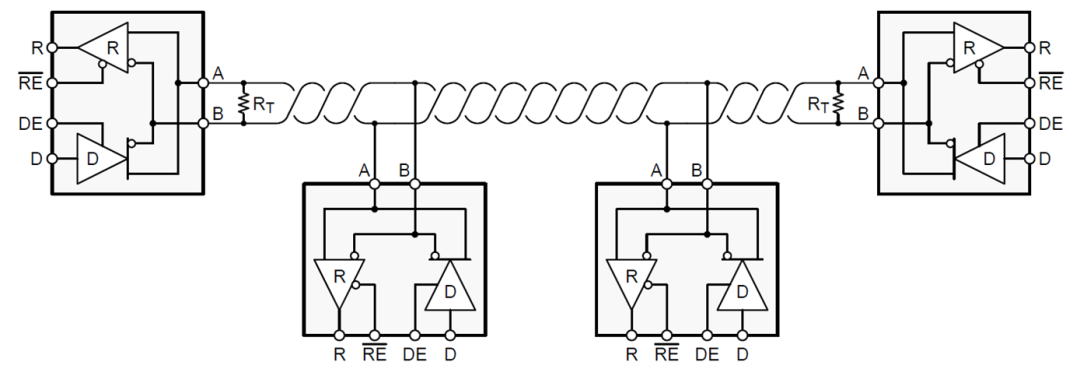
Figure 1: RS-485 Bus with Parallel Termination

What is fail-safe biasing and how to achieve it?

Fail-safe biasing is a way to ensure that the RS-485 receiver does not enter an indeterminate state due to differential input voltage. The Electronic Industries Alliance (EIA)-485 standard states: When the differential voltage ≥ +200mV, the RS-485 input threshold is logic high; when the differential voltage ≤ -200mV, the RS-485 input threshold is logic low, thus maintaining a 400mV indeterminate state between the high and low thresholds.
Fail-safe biasing can be achieved in two ways:
-
Choosing transceivers with built-in fail-safe input thresholds in the receiver.
-
Adding external resistors to create an external bias on the unconnected bus.
Both methods can ensure a logic high state on the bus.

How to calculate the maximum number of nodes on an RS-485 bus?

RS-485 is a multipoint differential bus, meaning all nodes on the bus share a common transmission medium. As the total number of nodes increases, the load on each driver will also increase.
The Telecommunications Industry Association (TIA)/EIA-485 standard creates a hypothetical unit load (UL) to help calculate the maximum number of nodes on the RS-485 bus. The standard states: Drivers must be able to drive at least 1.5V differential signals in parallel on up to 32 unit loads, with two 120Ω termination resistors connected at both ends of the bus.
Formula 1 shows the worst-case ratio of input voltage divided by leakage current to calculate input resistance. After determining the input resistance of the nodes, Formula 2 can be used to calculate the maximum number of nodes on the RS-485 bus:
Input Resistance = Maximum (VIN/I leakage) (1)
Number of Nodes = 32 / Input Resistance (2)

When is it necessary to add a ground wire between nodes?

When designing remote data links, it must be assumed that there are some ground potential differences. These voltages will add common-mode noise Vn to the transmitter output. Even if the total superimposed signal is within the common-mode range of the receiver, relying on local ground potential differences as a reliable path for return current is unsafe. When the ground potential difference (GPD) exceeds the common-mode range of the receiver (which often occurs in long cables and high-current loads), appropriate grounding techniques need to be used.
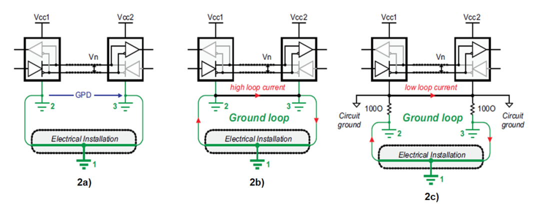
Figure 2: Remote Node Configurations: Independent Ground Point (a);
Directly Connected Remote Ground (b);
Separation of Device Ground and Local System Ground (c)
Figure 2a shows a remote node that may draw power from different parts of the electrical installation. Any changes to the installation (for example, during maintenance work) can cause the GPD to exceed the common-mode range of the receiver’s input. Therefore, it may cause the currently functioning data link to stop working in the future.
It is also not recommended to directly connect remote grounds via a ground wire (Figure 2b) because direct connections can cause large ground loop currents to couple as common-mode noise onto the data lines.
To achieve direct connection of remote grounding, the RS-485 standard recommends separating device grounding from local system grounding by inserting resistors (Figure 2c). While this method reduces loop currents, it makes the data link sensitive to noise generated elsewhere in the loop due to a large ground loop. Thus, a stable data link has not been established.
To withstand ground potential differences (GPD) of up to several thousand volts over a robust RS-485 data link, the best approach is to isolate the signal and power lines of the bus transceiver from its local signal and power. In this case, power isolators (such as isolated DC/DC converters) and signal isolators (such as digital capacitive isolators) can prevent currents from flowing between remote system grounds and avoid creating current loops.

What are the recommended values for RS-485 length and speed?

At the rated data rate, the maximum bus length is limited by transmission line loss and signal jitter. Due to jitter at baud rates of 10% or more, data reliability drops sharply, so Figure 3 shows the cable length versus data rate characteristics of traditional RS-485 cables under 10% signal jitter.
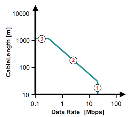
Figure 3: Recommended Cable Length versus Data Rate
In Figure 3, the circle labeled 1 represents the high data rate area when the cable length is short. Here, transmission line losses can be ignored. Data rate primarily depends on the rise time of the driver. Although the standard recommends using 10 Mbps, today’s fast interface circuits can operate at data rates of up to 50 Mbps.
The red circle labeled 2 represents the transition from short data lines to long data lines. Losses in longer transmission lines must be considered. Therefore, as the cable length increases, the data rate must be reduced. Empirically, the product of line length [m] and data rate [bps] should be 10 to the power of seven.
The red 3 represents the low-frequency range where the interaction between the cable’s series resistance and line termination leads to signal attenuation. At some point, the amplitude of the signal becomes smaller than the amplitude that the receiver can normally detect (i.e., not exceeding the VIT threshold).

How to estimate the power consumption of RS-485?

To calculate power consumption, power can be divided into several parts. When the device is powered on without external load, the power consumption will be used for the integrated circuit itself. If a load is added at the output pins, the power to drive the load will be drawn from the device. Since RS-485 has differential signals, loads are typically added between the A and B pins.
In Figure 4, the blue trace, PDic, is the power consumed by the device. For low data rates, power consumption mainly comes from resistive loads (red trace), PDdc. For high data rates, the power consumption of capacitive loads (green trace) PDac must be considered.
Figure 4: Power Consumption Calculation Sector
Formula 3 calculates total power consumption as:
PDtotal = PDic + PDdc + PDac (3)
To calculate total power consumption, the power of each part must first be calculated. Device power consumption is referenced in Formula 4, where the static supply current Icc is specified in the datasheet:
PDic = Vcc*Icc (4)
If a resistive load is placed on the bus, the driver will generate a voltage (Vod) across it, as shown in Formulas 5 and 6, where C is the parasitic capacitance, which includes the capacitance of the transceiver, the load capacitance, and the trace capacitance. The data frequency f is also included in the calculation.
PDdc = Vcc*I – I2*R = (Vcc – I*R)*I (5)
PDac = 2*2C*f*Vcc*Vod (6)

How to protect RS-485 interfaces from electrostatic discharge (ESD)?

There are various types of ESD protection, including human models, International Electrotechnical Commission (IEC) contact discharge, and IEC air gap discharge. If a transceiver is integrated with IEC ESD (such as Texas Instruments’ THVD1450 or THVD1500), the RS-485 interface can be protected from ESD at the specified transceiver levels without external components.
For example, THVD1450 can support 18-kV IEC 61000-4-2 contact discharge without any external components. Many devices on the market do not have this integration, therefore external transient voltage suppression (TVS) diodes are required.

How to know if an external TVS diode is needed?

Industrial networks must operate reliably in harsh environments. Electrical overstress transients caused by ESD, switching of inductive loads, or lightning can disrupt data transmission and damage bus transceivers, unless effective measures are taken to reduce transient effects.
Texas Instruments devices have been tested according to the following standards:
ESD immunity testing of IEC 61000-4-2, simulating operators directly applying static electricity to adjacent electronic components. THVD1500 and THVD1450 have passed this standard test.
Electrical fast transient (EFT) or surge immunity testing of IEC 61000-4-4, simulating everyday switching transients caused by inductive load interruptions, relay contact bounce, etc. THVD1450 and THVD1550 have passed this standard test.
In terms of current and duration, the surge immunity test IEC 61000-4-5 is the most stringent transient immunity test, lasting about 1000 times longer than ESD and EFT tests. THVD1429 and THVD1419 have passed this standard test.
Texas Instruments’ latest THVD series RS-485 transceivers integrate various levels of protection according to these standards without the need for additional external protection. The protection levels are specified in the device datasheet.

How to prevent high voltage short circuits?

In many RS-485 applications, there is a risk of accidentally connecting communication lines to power lines. This risk is particularly high in field-installed systems, such as HVAC systems, lighting control, or other building automation applications. In these cases, it is essential to ensure that RS-485 transceivers are not damaged to avoid costly field returns and reinstallation risks.
While clamping devices like TVS diodes can limit the maximum voltage seen by the transceiver during transient events, they often cannot prevent prolonged stress (e.g., DC short circuits). To prevent these situations, some series current-limiting components are needed. A typical approach is to use positive temperature coefficient (PTC) resistors. These resistors have a low resistance under nominal conditions, but under fault conditions, when a large current flows (such as through a TVS or other clamping devices), the resistance increases. Click to read the original article, Texas Instruments reference design “Protecting RS-485 Transceivers from Continuous High Voltage/Electrical Overstress Reference Design” shows an example of implementation using the THVD1500 transceiver.
However, using these additional series current-limiting and parallel voltage clamping components can be expensive and take up valuable PCB space. Therefore, in most cases, a more optimized approach is to use transceivers that can withstand these high fault voltages without external protection. THVD2450 is an example, rated to withstand DC short circuit voltages of up to +/- 70V.
Did this article miss anything? Please comment below, and we will send feedback to help you solve RS-485 design challenges.
For specific information on isolated RS-485 transceivers, please check the FAQ blog post: “Seven Questions about Isolated RS-485 Transceivers.”
Want to learn more about RS-485? Scan the QR code below, to enter the TI Precision Lab! Surprises await you!


Click “Read the original article”, to see examples of implementation using the THVD1500 transceiver.