“Analyzing the working principles of digital-to-analog converters and analog-to-digital converters—from resistor ladder networks to Delta-Sigma modulation techniques.”
 Microcontrollers are “consuming” the entire world. Nowadays, even the most basic tasks like blinking an LED are cheaper and simpler with microcontrollers than building oscillating circuits with discrete components or relying on the once ubiquitous 555 timer chip.
However, in this increasingly software-defined world, 0s and 1s are not omnipotent. Image sensors record light intensity as a series of analog values; speakers playing music require their diaphragms to move to various positions beyond just “fully in” and “fully out.” Ultimately, almost all complex digital circuits require dedicated digital-to-analog converters (DACs) and analog-to-digital converters (ADCs) to connect to the physical world. These converters are often integrated into the microcontroller’s chip, but their principles are still worth exploring.
Simple Digital-to-Analog Converter (DAC)
The core of converting digital signals to analog signals lies in mapping a fixed-length binary number to a quantized output voltage range. For example, a 4-bit DAC has 16 possible output voltages, which behave as follows:
0000 (0) = 0 V 0001 (1) = 1/15 Vdd 0010 (2) = 2/15 Vdd 0011 (3) = 3/15 Vdd ... 1111 (15) = Vdd The simplest way to implement such conversions is based on a resistor-weighted binary DAC: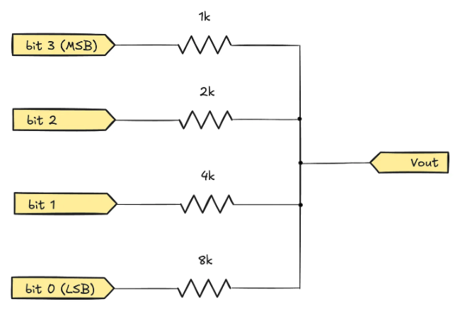
Clearly, when the binary input is 0000, the analog output should be 0V; conversely, if the input is 1111, the output must reach Vdd. For intermediate input values, we should obtain a weighted average of the resistors, where the influence weight of each bit is half that of its higher-order bits. This characteristic perfectly aligns with how binary numbers operate.
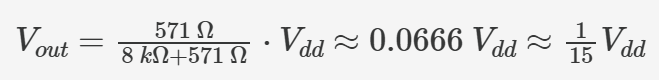
We can conduct a more rigorous circuit analysis. Taking the input value 0001 as an example: at this point, the three higher-order resistors (bits #1, #2, and #3) are connected in parallel to ground, and their equivalent resistance is:
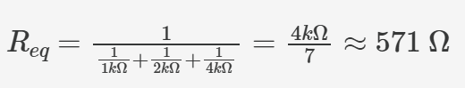
Meanwhile, the resistor corresponding to the least significant bit (LSB) is connected to Vdd. The entire circuit can be viewed as a voltage divider network consisting of two series resistors from Vdd to ground, with the output voltage given by:
Similarly, when the input is 1110 (decimal 14), the output voltage Vout ≈ 14/15 Vdd. This aligns perfectly with our expected linear response characteristics.
The main drawback of this DAC architecture is that the required resistor values quickly become impractical. To avoid excessive static current, the resistor value corresponding to the most significant bit (MSB) cannot be too low (1 kΩ is a reasonable starting value). However, for a 16-bit DAC, this means the least significant bit resistor must reach 1 kΩ × 2¹⁵ ≈ 32 MΩ; if achieving 24-bit resolution, resistors in the gigaohm (GΩ) range are required. Manufacturing such high-precision large-value resistors on integrated circuit wafers is extremely challenging, especially if they are to have the same temperature coefficient.
To address this issue, engineers have proposed a clever R-2R ladder DAC architecture solution:
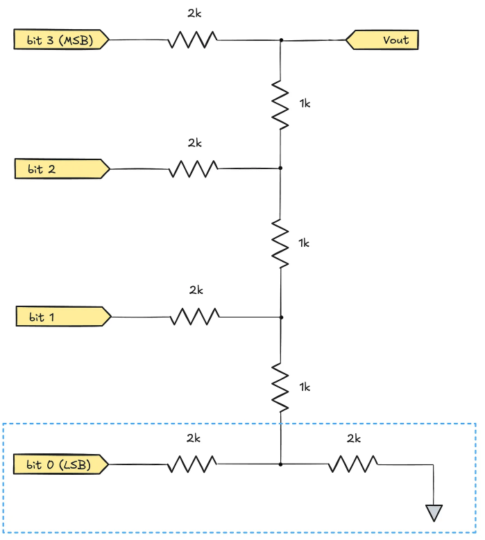
Compared to traditional architectures, this R-2R ladder circuit is not as intuitive, but its working principle is similar. To analyze its design logic, we start from the lowest structural level: the two horizontally placed resistors at bit #0. These two resistors provide equal current to the rest of the circuit, thus functioning equivalently to a 1 kΩ resistor connected to the synthesized input voltage. The value logic of this synthesized voltage is: when LSB=0, it equals 0V; when LSB=1, it equals Vdd/2. In other words, the input signal at bit #0 is compressed to a 50% weight here.
Through this equivalent substitution, we obtain the simplified circuit shown on the left. Further observation reveals that the two series 1 kΩ resistors (marked in red) in the lower structure can be equivalently replaced by a single 2 kΩ resistor in the right diagram:
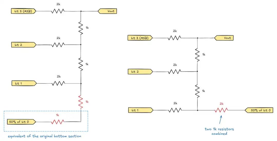
At this point, we can see that the configuration of bit #1 in the new circuit is similar to the previous analysis of bit #0. Its lower structure includes a 2 kΩ resistor connected to the corresponding binary input and another 2 kΩ resistor connected to the previous synthesized voltage. In fact, this structure achieves a 50% mixing effect of the two signals. Regardless of how the upper circuit changes, this part can be equivalently replaced by a single 1 kΩ resistor connected to the new synthesized input signal:
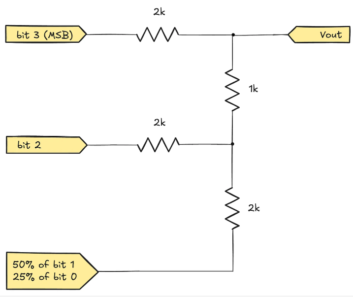
This iterative process can continue. Ultimately, it can be clearly derived that the output voltage will be contributed by bit #3 at 50%, bit #2 at 25%, bit #1 at 12.5%, and bit #0 at 6.25%.
(It should be noted that the sum of the above weights does not reach 100% because the initial pull-down resistor at the bottom of the ladder structure will dissipate some voltage range.)
Oversampling DAC
Although the architecture discussed above is simple and elegant, it faces linearity challenges in high-resolution scenarios (especially beyond 10-12 bits). While the precision of resistor components can reach 0.1% levels, in a 16-bit DAC, the theoretical influence weight of the least significant bit (LSB) is only 0.003% of that of the most significant bit (MSB). If the MSB resistor value deviates by 0.1% from the design value, it is enough to severely degrade the linearity of the entire system.
This dilemma has led to the development of oversampling average DACs. Such devices output low-resolution alternating signals at high frequencies and then use a low-pass filter at the output to average the signals, generating finer low-frequency intermediate voltages.
For example, averaging four consecutive single-bit DAC outputs can insert three intermediate voltage values between the native output range, effectively achieving a two-bit effective precision improvement:
average(0,0,0,0)=0average(0,0,0,1)=0.25average(0,1,0,1)=0.5average(0,1,1,1)=0.75average(1,1,1,1)=1Of course, this solution comes at a cost: some high-frequency noise may not be completely suppressed by the filter. Nevertheless, this approach is overall quite robust. In fact, many DACs in consumer audio devices use single-bit pulse sequences (operating at frequencies of hundreds of thousands of hertz) to achieve the claimed 24-bit output resolution. Although the inherent noise of the circuit often limits the practical significance of this metric, single-bit DACs exhibit excellent linearity performance—because precise timing control is much easier to achieve than manufacturing ultra-precise resistors.
Classic Analog-to-Digital Converter (ADC)
Compared to digital-to-analog conversion, the process of converting analog voltage to binary numbers is more complex. To achieve precise instantaneous voltage quantization, the only practical method is to configure independent voltage comparators (open-loop operational amplifiers) for each quantization level, for example:
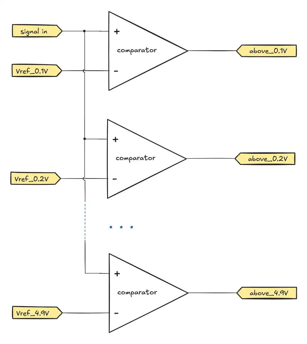
Parallel comparator ADCs (also known as “flash” ADCs) are occasionally used in special scenarios requiring extreme speed, but their circuit scale grows exponentially with the number of bits—leading to a dramatic deterioration in chip power consumption, input capacitance, and other parameters. Therefore, the resolution of such ADCs typically does not exceed 4-8 bits.
A more common architecture employs a single comparator working in conjunction with a predictable varying reference voltage. A basic example is a circuit that charges a capacitor through a resistor: by measuring the time interval from the start of charging to the comparator trigger, the input voltage value can be inferred.
In practice, due to the nonlinear characteristics of the capacitor’s constant voltage charging curve, an integrator circuit is usually used to generate the reference signal:
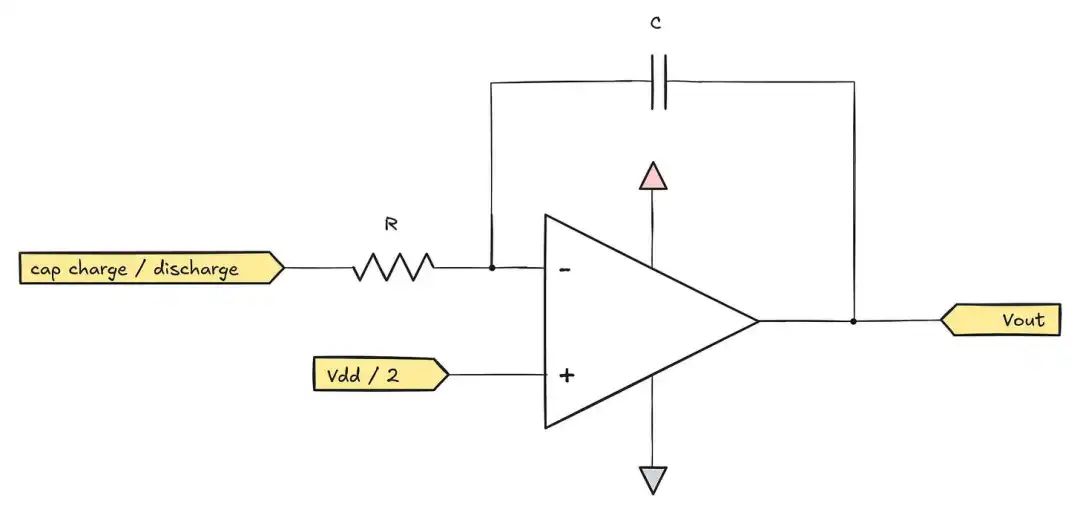
The integrator introduces an interesting tweak in standard op-amp circuits: replacing the conventional feedback resistor with a feedback capacitor. When the inverting input voltage (Vin-) exceeds the non-inverting input (Vin+), the op-amp output voltage immediately drops, allowing the charging current to flow through resistor R to charge the capacitor.
The core of this feedback mechanism is to maintain equal potentials at Vin- and Vin+. According to Ohm’s law, with a fixed input resistance, the charging current is determined solely by the input voltage and resistor R. When the charging current is constant, the capacitor voltage rises linearly. If a square wave signal is input, the integrator will output an almost perfect triangular wave, providing an extremely ideal linear reference signal for the ADC.
The time interval from the start of charging to the comparator trigger depends not only on the input voltage but also on the slope of the triangular wave, which is itself constrained by the precision of R and C parameters. To improve accuracy, the ADC needs to measure the duty cycle of the comparator output signal over multiple cycles of the triangular wave. For example, a 25% duty cycle means the measured voltage is at 75% of Vdd, and this measurement result is independent of the precision of R and C.
ADC based on slope integration has high precision and low noise advantages, but suffers from slow conversion speeds. A performance-optimized solution is to use digital assist technology: the successive approximation register (SAR) architecture. Its core principle is to generate a reference voltage using an internal DAC and execute an algorithm similar to binary search in computer science: first comparing the input voltage with Vdd/2, if the input is higher, the lower half of the range is excluded, and then the next comparison is made at the midpoint of the remaining range (3/4 Vdd). By successively halving the search range, only a few iterations are needed to lock in the precise value. The trade-off is that there is a loss of accuracy due to the linear error of the DAC, and digital switch noise increases somewhat.
High-end (“pipeline”) ADCs often adopt multi-technology fusion solutions: for example, quickly determining part of the high bits through a “flash” ADC architecture, and then obtaining more low bit data through multi-stage scaling and conversion processing.
Delta-Sigma (Δ-Σ) ADC
At this point, ADC technology has shown diverse implementation paths, but the most ingenious solution is the high-frequency interpolation method, typically using Δ-Σ (Delta-Sigma) modulation technology. Its working mechanism is quite unconventional.
A basic 1-bit Δ-Σ ADC outputs high-speed “0” or “1” logic pulse sequences through a comparator stage. These digital outputs are fed into a special feedback loop to calculate the difference between the binary output and the input signal:
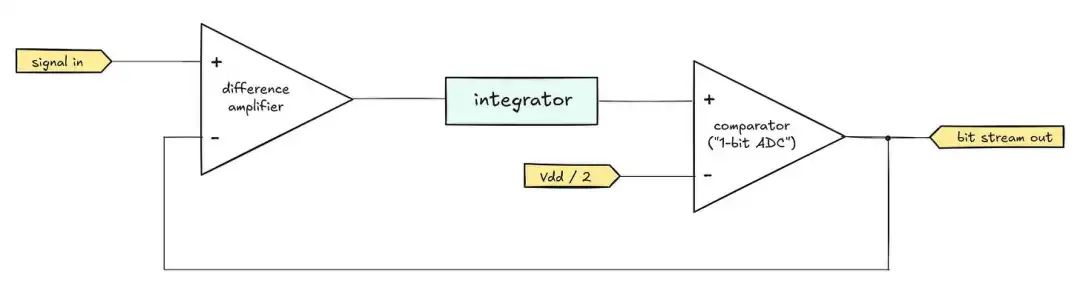
Simplified 1-bit Δ-Σ ADC architecture diagram (clock signal omitted)
In most cases, the analog input voltage does not equal the two possible voltage values of the digital output, so the operational amplifier with a gain of 1 at the front end of the Δ-Σ ADC (left diagram) will output instantaneous large positive or negative error voltages.
These instantaneous errors are then input to the integrator. As mentioned earlier, the integrator accumulates the error by integrating over time (storing the cumulative value in a linearly charging capacitor). If the input signal positively deviates from the average of the pulse sequence, the integrator output voltage will gradually rise; conversely, it will gradually fall.
This accumulated error ultimately inputs to the positive terminal comparator that generates the actual output bit stream. The core logic is: if the error is positive (i.e., the ADC outputs “0” too much), the comparator will force an output of “1”; conversely, if the accumulated error is negative (too many outputs of “1”), it will switch to output “0”:
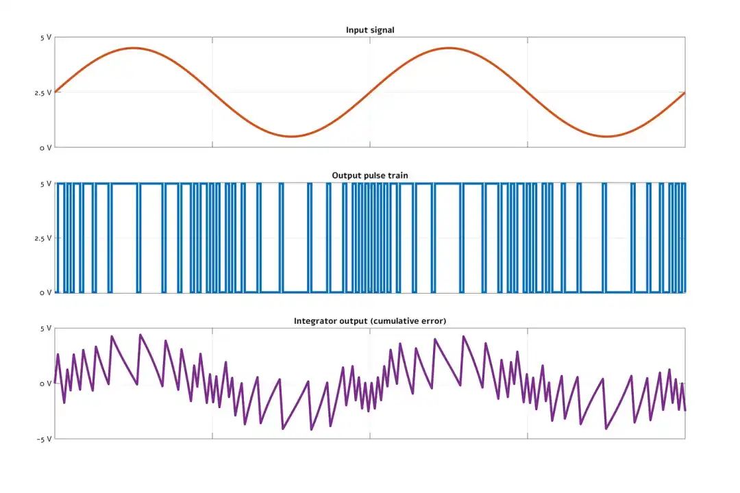
Typical working waveform of a first-order Δ-Σ ADC
Although this measurement method seems irrational, the duty cycle of the seemingly chaotic high-frequency pulses can accurately infer the analog input value through digital processing. The greatest advantage of this architecture is that there are very few sources of analog error, resulting in excellent linearity performance. The trade-off is that to achieve reasonable accuracy, the ADC’s operating clock frequency must be much higher than the target sampling rate.
It should be particularly noted that the term “Δ-Σ” is also used to refer to the oversampling interpolation DAC subclass mentioned earlier. However, compared to ADCs, these DACs have significantly lower intelligence: their pulse modulation mainly occurs in the digital domain, lacking the sophisticated analog feedback mechanism.
Original text reproduced from:https://lcamtuf.substack.com/p/dacs-and-adcs-or-there-and-back-again, translated and verified
Note: If you want to receive KiCad content updates first, please click the card below, follow, and then set it as a star.
Common collection summary:
-
Learn KiCad with Dr. Peter
- KiCad 8 Exploration Collection
- KiCad Usage Experience Sharing
- KiCad Design Projects(Made with KiCad)
- Common Problems and Solutions
- KiCad Development Notes
- Plugin Applications
- Release Records