To address the limitations of flatPCBs in integration, heat dissipation, positioning, etc., cavities are often set on their surfaces to achieve miniaturization and high performance of electronic products. Based on the structural characteristics of the cavities, they can be divided into three categories:
(1) Cavities with no metal layer on the bottom or side walls
This type of cavity is commonly used to install taller components, embedding them partially or entirely within thePCB to achieve a thinner electronic product (low profile). Alternatively, they can be used for concave-convex positioning with structural components (enclosures, brackets, etc.), reducing the use of fasteners.
Due to misalignment between core boards or compensation for semi-cured sheet retraction, unpressed gaps (not delamination) may occur, allowing the distance from the cavity to the nearest conductor to be reduced by ≤50%, with a maximum reduction not exceeding 0.25 millimeters, taking the smaller of the two values. This regulation also applies to the second type of cavity.
(2) Cavities with one or more metal layers on the bottom or side walls
In RF circuits, this type of cavity can form a structure that transitions from stripline to microstrip, thereby achieving a nearly planar cascade and reducing the impact of cascade height differences on electrical performance.
In applications involving high-power components, the bottom of this type of cavity can be made of copper, aluminum, molybdenum-copper, or other metals with high thermal conductivity, or filled with conductive paste in large area via metal layers. High-power components installed in the cavity make direct contact with the metal for efficient heat dissipation, avoiding inefficient operation or burnout of the components.
Conductors extending from the side walls of the cavity and continuous at the bottom allow a maximum size of0.75mm for overflow of the semi-cured sheet onto the conductor. For pads located at the bottom of the cavity and within 0.75 millimeters from the side wall of the cavity, the overflow of the semi-cured sheet should be determined by AABUS.
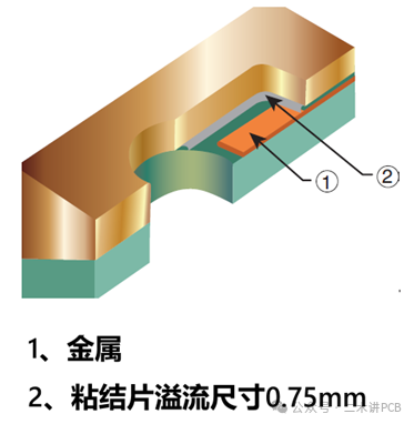
Figure1 Cavities with metal layers on the side walls or bottom
(3) Cavities with continuous metal layers on the bottom and side walls
This type of cavity has continuous metal layers on both the bottom and side walls, commonly used to achieve electromagnetic shielding for sensitive components, reducing electromagnetic interference from surrounding circuits.
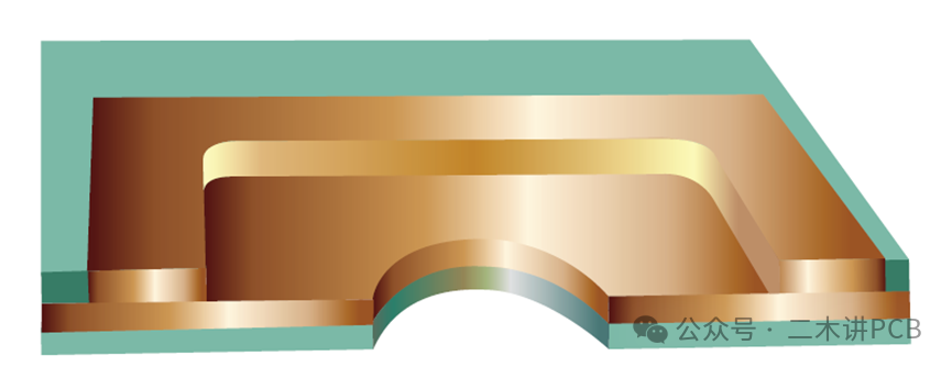
Figure2 Schematic of a fully metal cavity
For cavities with a conductive layer on the bottom that require soldering or wire bonding (excluding the area where overflow of the semi-cured sheet is allowed), the intact area is defined as60% of the center area of the feature profile (circular, rectangular, square, etc.). For cavities with a coating on the side walls, the coating and voids on the side walls must not exceed the allowable range specified inTable 1. Each side wall of the coated cavity should be evaluated separately, and the total area of multiple voids on the same side wall must not exceed the specified percentage of area.
Table1 Requirements for voids in the metal layer of cavity side walls
|
Material |
Level 1 |
Level 2 |
Level 3 |
|
Copper |
Side wall void area ≤20%; Void size ≤ 60% of side wall length or height |
Side wall void area ≤10%; Void size ≤ 40% of side wall length or height |
Side wall void area ≤5%; Void size ≤ 20% of side wall length or height |
|
Coating |
Side wall void area ≤20%; Void size ≤ 60% of side wall length or height |
Side wall void area ≤10%; Void size ≤ 40% of side wall length or height |
Side wall void area ≤5%; Void size ≤ 20% of side wall length or height |