When TSMC announced the mass production of 2nm process in the second half of 2025, and ASML’s EUV lithography machines firmly occupied the core of the high-end equipment market, the Chinese semiconductor industry stood at a critical juncture, transitioning from “local breakthroughs” to “full-chain collaboration.” The global semiconductor market is expected to reach a scale of $705 billion in 2025, with a growth rate exceeding 15%, marking a structural recovery driven by demand from AI servers and new energy vehicles. However, in the geopolitical restructuring of a “tripartite balance” (USA 44%, East Asia 41%, EU 10%), mainland China, despite holding only a 5% share, is achieving a growth rate higher than the global average, creating breakthroughs in mature processes, advanced packaging, and new materials.

1. Global Recovery and Supply Chain Restructuring: China’s “Crisis” and “Opportunity”
The year 2025 for the global semiconductor industry will be one of explosive demand and high barriers. According to Gartner data, the shipment volume of AI servers is expected to surge by 30% year-on-year, with the number of chips used in new energy vehicles exceeding 1,500, driving a boom in demand for high-end GPUs and power semiconductors. The storage market, following an 81% growth in 2024, is expected to maintain double-digit growth in 2025, with new types of memory like HBM being in high demand. However, at the same time, the U.S. CHIPS Act with $52.7 billion in subsidies and the EU’s €43 billion industrial investment, combined with escalating technology restrictions on China, are pushing the supply chain towards “regionalization + diversification,” making it increasingly difficult for Chinese companies to acquire advanced equipment and IP cores.
However, the unique advantages of the Chinese market are becoming the foundation for breakthroughs. As the world’s largest semiconductor consumer market, China’s market size is expected to exceed 1.3 trillion yuan in 2025, with demand from AI computing power and the industrial internet providing a “trial and error” space for local enterprises. On the policy side, the “Big Fund” Phase III with 344 billion yuan is being implemented, and local governments like Shenzhen are supporting with 5 billion yuan in private equity funds, accelerating the concentration of resources in critical areas like equipment and materials. On the capital side, the acceleration of IPO reviews and active mergers and acquisitions, such as SMIC’s acquisition of subsidiary equity and Huahong’s capacity expansion, are driving the concentration of industrial resources towards leading enterprises.
2. Breakthroughs in the Industry Chain: From “Single Point Breakthrough” to “Cluster Assault”
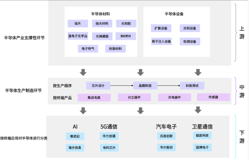
The breakthroughs in the Chinese semiconductor industry chain have shifted from “single point flashes” in individual segments to “cluster efforts” across multiple fields. In manufacturing, SMIC’s 14nm process is stably mass-produced, and the N+1/N+2 processes are entering practical stages. By 2025, the 12-inch wafer capacity is expected to rank first globally, with the share of mainstream processes from 22nm to 40nm potentially reaching 42% by 2028, becoming a core supplier of global mature process capacity. In the packaging and testing field, companies like JCET and Tongfu Microelectronics have entered the global top three, using advanced Chiplet packaging technology to meet the high bandwidth memory demands of AI large models, with the Chinese packaging and testing market expected to exceed 120 billion yuan by 2025.
The “ice-breaking” in supporting segments is particularly crucial. On the equipment side, AMEC’s 5nm etching machine has received certification from international manufacturers, and SSMC’s Shanghai coating and developing equipment has broken the overseas monopoly. North Huachuang’s 28nm etching machine has entered mass production, with the Chinese semiconductor equipment market expected to exceed $50 billion by 2025, and the localization rate is projected to soar from 20% to over 60%. On the materials side, companies like Lianon and Shanghai Silicon Industry are accelerating capacity expansion, with the localization rate of 12-inch silicon wafers exceeding 50%. Tianyue Advanced’s 8-inch silicon carbide substrate yield exceeds 80%, and they have launched 12-inch silicon carbide substrate products, enhancing the energy efficiency of power devices in new energy vehicles by over 15%.
However, the gap in core areas cannot be ignored. EDA tools and IP cores remain highly dependent on imports, with the self-sufficiency rate of high-end lithography machines below 30%. The gap in advanced processes of 7nm and below compared to TSMC and Samsung still requires 5-10 years of technological accumulation, and these “bottleneck” areas remain core challenges for the Chinese semiconductor industry.
3. Technological Race: “Opportunity for Change” in Architecture and Materials
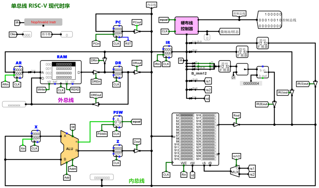
In the competition for advanced processes, China is seeking “opportunities for change” in technological architecture and new materials. The RISC-V architecture has become a key breakthrough point, allowing Chinese companies to bypass the patent barriers of traditional architectures due to its open-source and modular advantages. Companies like BittWare and Moore Threads are developing dedicated AI chips based on RISC-V, while Huawei’s Ascend series holds a 15% market share in the intelligent computing power market. It is expected that by 2027, the shipment volume of RISC-V chips will exceed 10 billion units, accounting for over 30% of the global market, establishing a self-controllable ecosystem.
The application of third-generation semiconductor materials opens up new scenarios. Silicon carbide (SiC) and gallium nitride (GaN) have advantages in high-voltage and high-temperature environments, making them core components in new energy vehicles and the low-altitude economy. In 2025, the Chongqing Low Altitude Economy Co-Insurance Body will be established, with the first batch of project risk coverage reaching 61.15 million yuan. It is expected that by 2035, the scale of this field will exceed 3.5 trillion yuan, providing a broad market for silicon carbide devices. In the new energy vehicle sector, the penetration rate of silicon carbide power devices is expected to exceed 40% by 2028, and breakthroughs in substrate manufacturing are driving the industry chain from “following” to “leading.”
4. Path to Breakthrough: Long-termism and Open Collaboration
The semiconductor competition in 2025 is no longer a contest of individual enterprises or single segments, but a competition of the entire industry chain ecosystem and long-term technological investment. To break through the “bottlenecks,” the Chinese semiconductor industry must avoid the impatience of “short-term sprints” and abandon the misconception of “closed-door manufacturing.” On the policy level, it is necessary to continue focusing on core areas such as EDA and high-end lithography machines, promoting industry-university-research collaboration through a “ranking mechanism.” On the market level, leveraging local demand advantages from AI computing power and new energy vehicles can provide “application scenarios” for technological iteration. On the international cooperation level, it is essential to integrate into the global supply chain with an open attitude, breaking through blockades through technological exchanges and collaborations while strengthening the resilience of the local supply chain.
From the global race for 2nm processes to the ecosystem construction of RISC-V architecture, the Chinese semiconductor industry is seeking a foothold in global competition with the strategy of “building a foundation with mature processes and breaking through with advanced technologies.” The year 2025 is not the end, but the starting point for “full-chain collaboration” — only by solidifying the foundation through independent innovation and breaking barriers through open cooperation can we truly achieve a leap from “catching up” to “leading” in the trillion-dollar semiconductor race.
Content Source: Network
This issue’s editor: Xiao Ai Business cooperation: 021-37709287Submission email: [email protected] (Accepted submissions will be compensated as agreed or noted with the source and a brief introduction of the submitter)
Copyright Statement: SCF respects copyright and appreciates the hard work and creativity of every author; except for articles that cannot be traced, we have noted the source at the end of the article; if there are copyright issues with articles, videos, images, or text, please contact us immediately, and we will confirm copyright based on the materials you provide and pay compensation according to national standards or delete the content immediately!