In today’s rapidly advancing technological era, semiconductors have become the core force driving transformation and progress across various industries. From the smartphones and computers we use daily to industrial automation equipment, automotive electronics, and cutting-edge aerospace and artificial intelligence applications, semiconductors are ubiquitous. Supporting all of this is a vast and complex semiconductor industry chain.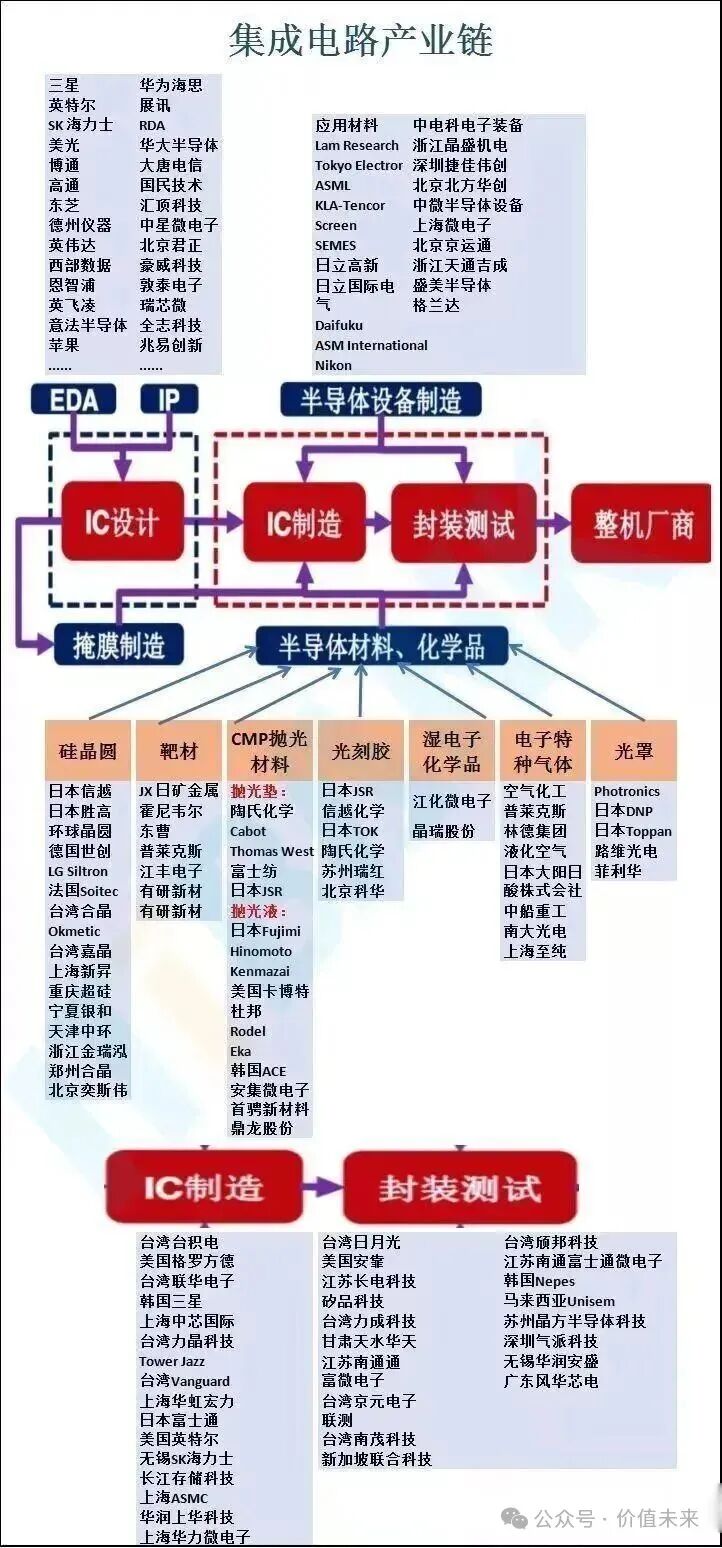 Upstream: Raw Materials and Equipment – The Foundation of the Industry
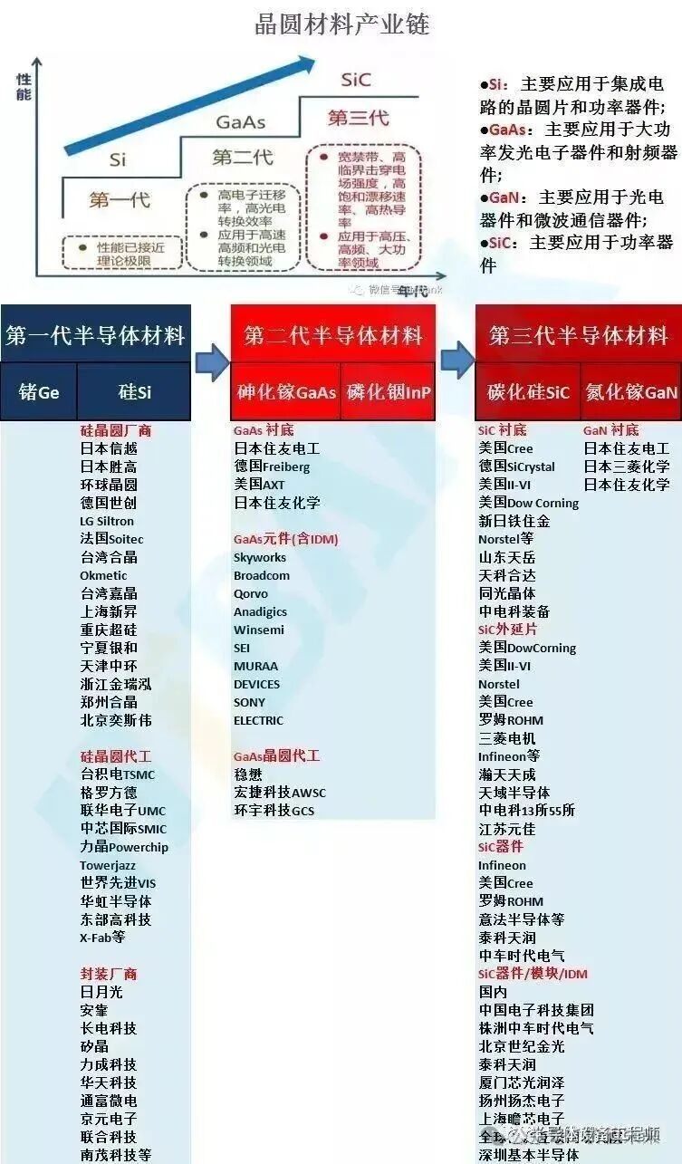
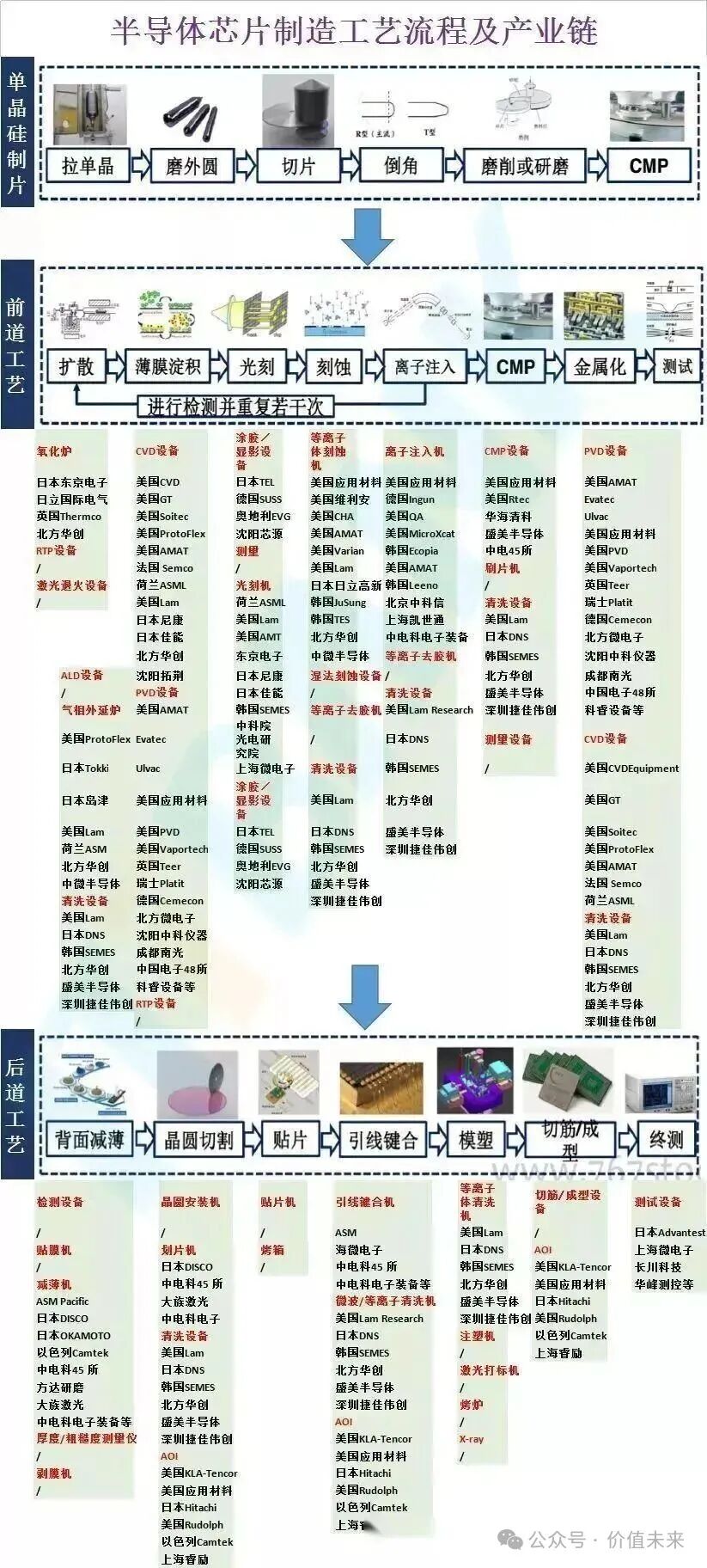
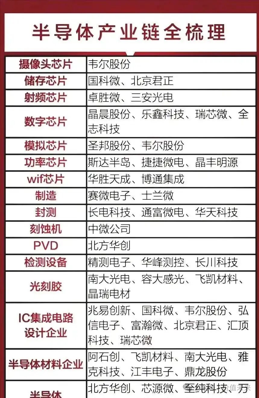
The upstream of the semiconductor industry chain consists of raw materials and equipment supply, which is the foundation of the entire industry. In terms of raw materials, silicon wafers are the most critical. Silicon, as a semiconductor material, possesses unique electrical properties, and high-purity silicon wafers undergo complex processing to become the basic carrier for chip manufacturing. In addition to silicon wafers, materials such as photoresists, specialty gases, and target materials also play indispensable roles in the chip manufacturing process. Photoresists are used to form fine circuit patterns on the wafers, specialty gases participate in various chemical reactions, and target materials are utilized in processes such as thin film deposition.
Downstream: Packaging, Testing, and Applications – Industry Extension
The downstream packaging, testing, and application segment is an extension of the semiconductor industry chain. Packaging protects the manufactured chips and provides interfaces for connection to external circuits. Packaging not only protects chips from external environmental influences but also affects chip performance and heat dissipation. With the continuous development of chip technology, packaging technology is also advancing, from traditional DIP packaging to today’s BGA, Flip Chip, and 3D packaging, with increasing packaging density and performance.
Note: The following content does not constitute any investment advice, guidance, or commitment, and is for discussion purposes only.
Upstream: Equipment and Materials (Core Battlefield for Domestic Substitution)
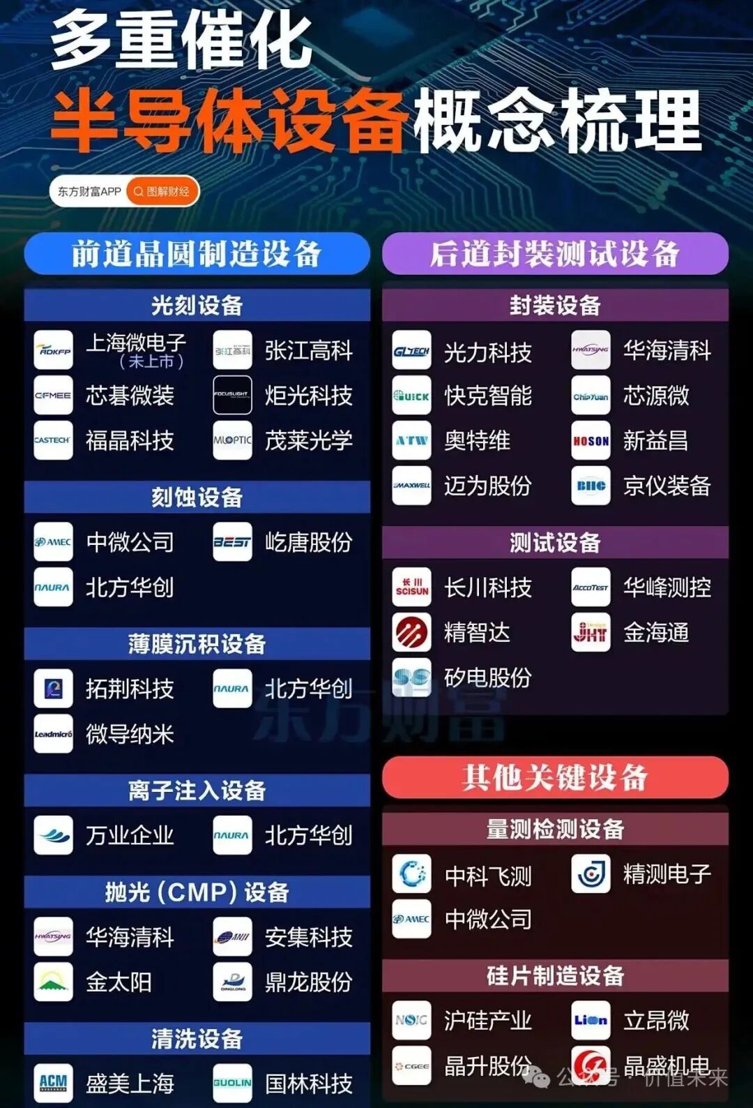
1. Semiconductor Equipment
Etching Equipment
Advanced Micro-Fabrication Equipment:5nm etching machine validated by TSMC, ranked in the top ten globally, with the 12-inch edge etching equipment Primo Halona™ set to be released in 2025, increasing capacity by 30%, with etching uniformity error < 0.5nm.
North Huachuang:Etching equipment accounts for over 30% of purchases by SMIC and Yangtze Memory Technologies, with a 90% verification rate for CCP etching equipment in logic chip production lines.
Thin Film Deposition Equipment
Topwin Technology:PECVD equipment holds a 15% market share in Yangtze Memory’s 128-layer 3D NAND production line, with advanced process equipment accounting for 35% of new orders in 2025.
Shengmei Shanghai:Orders for furnace tube equipment (LPCVD/ALD) continue until Q4 2025, with electroplating equipment performance increasing by 50% year-on-year, and supercritical CO₂ drying and cleaning equipment saving 50% in CO₂ usage.
CMP Equipment
Huahai Qingke:Domestic CMP equipment market share of 40%, with Universal-300 series critical dimension uniformity (CDU) < 0.5nm, and the second phase project set to double production capacity to 200 units/year by 2025.
Ion Implanters
Wanye Enterprises:Kaistone low-energy high-current equipment has a daily capacity of 3200 wafers, with cumulative shipments exceeding 5 million wafers, entering the supply chain of SMIC and Changxin Memory.
Testing Equipment
CASIC:Optical testing equipment fills a gap, with revenue of 702 million yuan in the first half of 2025 (up 51.39% year-on-year), and losses narrowing to 18.35 million yuan.
Changchuan Technology:Testing machines and probe stations are complementary, with revenue of 2.167 billion yuan in the first half of 2025 (up 41.80% year-on-year), achieving breakthroughs in SoC testing machines and memory testing machines.
2. Semiconductor Materials
Silicon Wafers
Shanghai Silicon Industry:Leading domestic supplier of 12-inch silicon wafers, supplying SMIC and TSMC, planning to acquire subsidiaries such as Xinxing Crystal Investment for 7.04 billion yuan in 2025 to strengthen the entire chain capability of crystal pulling, cutting, grinding, and polishing.
Liang Micro:Market share of over 30% for automotive-grade silicon wafers, with 6-inch silicon carbide-based gallium nitride products passing customer validation, set for mass production in the second half of 2025.
Photoresists
Nanda Optoelectronics:ArF photoresists validated by SMIC, a key breakthrough in domestic substitution, with a global market share of over 60% for MO sources.
Tongcheng New Materials:Subsidiary Beijing Kehua’s KrF photoresists hold the top domestic market share, with ArF photoresists in mass production and introduced to Yangtze Memory, achieving self-sufficiency in KrF/ArF photoresist materials through self-developed resins.
Electronic Specialty Gases
Huate Gas:The only domestic supplier of photoresist gases certified by ASML, with 55 products achieving import substitution and 20 products entering 14nm/7nm production lines.
China Shipbuilding Specialty Gases:Second in global capacity for nitrogen trifluoride, first in global capacity for tungsten hexafluoride, with photoresist gases (Kr/Ne, Ar/Ne/Xe) certified by Japan’s GIGAPHOTON.
CMP Materials
Anji Technology:Polishing slurry domestic substitution rate exceeds 50%, with revenue of 1.835 billion yuan in the first half of 2025 (up 48.24% year-on-year), compatible with 14nm logic chips and 128-layer 3D NAND.
Dinglong Co., Ltd:Polishing pads break Dow’s monopoly, with plans to expand market share in 2025, increasing CMP materials revenue share to 35%.
Target Materials
Jiangfeng Electronics:High-purity sputtering target materials cover 28-7nm nodes, with 5nm products entering TSMC’s supply chain, planning to raise 1.948 billion yuan in 2025 to expand production of electrostatic chucks and Korean target material bases.
ASMC:Molybdenum target materials hold a global market share of 33%, with 12-inch wafer target materials entering Yangtze Memory’s supply chain, and photovoltaic target materials supplied to LONGi and Tongwei.
Midstream: Design and Manufacturing (The Segment with the Highest Technical Barriers)
1. Chip Design
AI Chips
Cambricon:The Siyuan series NPU computing power is close to NVIDIA’s H20, winning a bid for a certain state-owned bank’s thousand P-level computing project, with revenue growth of 300% year-on-year in the first half of 2025.
Haiguang Information:Leading domestic x86 CPU manufacturer, with DCU chip performance close to NVIDIA’s A100, receiving significant investment from the big fund’s third phase, with server chip shipments exceeding 500,000 units in 2025.
Memory Chips
GigaDevice:NOR Flash ranks among the top three globally, with automotive-grade DRAM in mass production, set to launch 1Gb SPI NOR Flash supporting 55nm process in 2025.
Lanqi Technology:DDR5 memory interface chips hold a global market share of 60%, with plans to launch PCIe 5.0 Retimer chips in 2025, compatible with AI servers.
RF Chips
Zhuosheng Micro:5G RF switch domestic substitution rate exceeds 70%, with plans to launch RF modules supporting Sub-6GHz frequency bands in 2025, supplying Xiaomi and vivo.
San’an Optoelectronics:Leading in third-generation semiconductor RF devices, with GaN-on-SiC HEMT devices applied in base stations and radar, with production capacity set to increase to 100,000 units/year in 2025.
Automotive-grade Chips
Weir Shares:Leading global market share for automotive CIS, with plans to launch an 8MP front-facing camera chip in 2025, compatible with L3+ autonomous driving.
2. Wafer Manufacturing
Mature Processes
SMIC:Ranked first globally in 28nm capacity, with automotive-grade chip revenue accounting for 40%, planning capital expenditures exceeding 50 billion yuan in 2025, focusing on expanding mature process capacity.
Huahong:Leading in specialty process foundry, with embedded storage technology at the forefront, with revenue growth of 23% year-on-year in Q2 2025, and capacity utilization exceeding 90%.
Advanced Packaging
Changdian Technology:The third-largest packaging and testing factory globally, with CoWoS packaging in mass production, achieving breakthroughs in HBM stacking technology, with advanced packaging revenue accounting for over 60% in 2025.
Tongfu Microelectronics:Key player in packaging and testing for AMD’s 5nm chips, with Chiplet technology holding the top domestic market share, and capacity utilization exceeding 85% in 2025.
Downstream: Applications and End-Users (Explosive Growth in Demand)
1. Smart Vehicles
Power Devices
StarPower:Automotive-grade IGBT module domestic substitution rate exceeds 20%, with plans to launch 1200V SiC MOSFET in 2025, compatible with 800V high-voltage platforms.
Times Electric:Rail transit IGBT market share exceeds 60%, supplying automotive-grade IGBT modules to BYD and NIO, with production capacity set to increase to 500,000 units/year in 2025.
Sensors
Micron:Leading domestic MEMS microphones, with plans to launch automotive-grade pressure sensors in 2025, passing AEC-Q100 certification.
Four-Way Optoelectronics:Gas sensors supporting Tesla, with breakthroughs in gas analysis modules for LiDAR, with orders expected to grow by 150% in 2025.
2. AI and Cloud Computing
Server Chips
Inspur:Among the top three in AI server shipments, with liquid-cooled data centers achieving a PUE as low as 1.12, participating in the construction of 80% of national intelligent computing centers.
Topway Information:Core partner of Huawei Ascend, with “Zhaohan” servers compatible with various large models, with orders exceeding 3 billion yuan in 2025.
Optical Modules
Inspur Technologies:Mass production of 800G silicon optical modules, supplying NVIDIA and Amazon, with production capacity exceeding 1 million units in 2025.
Tianfu Communication:Leading in optical engine technology, with a 30% increase in AWG chip integration, with overseas revenue accounting for over 70% in 2025.
In summary, the current domestic substitution in the semiconductor industry chain has entered a critical stage of “equipment and material breakthroughs → design and manufacturing upgrades → application scenarios expanding,” with upstream equipment and materials, midstream AI chip design, and downstream smart vehicle applications being core investment directions. It is recommended to focus on leading enterprises with clear policy support, high technical barriers, and strong performance certainty.
*Disclaimer: This article is created by the original author. The content reflects their personal views, and our reprint is for sharing and discussion purposes only, not representing our endorsement or agreement. If there are any disputes or infringements, please contact us for removal!