
Previous articles mainly focused on the Processing System (PS) of the Zynq SoC, including:
- Using MIO and EMIO
- The interrupt structure of Zynq SoC
- Zynq private timers and watchdogs
- The triple timer counter (TTC) of Zynq SoC
However, from a design perspective, the truly exciting aspect of the Zynq SoC is creating applications that utilize the Zynq Programmable Logic (PL). Offloading tasks from the PS to the PL recovers processor bandwidth for other tasks, thereby accelerating operations. Additionally, the PS can control the operations executed by the PL in classic system-on-chip applications. Utilizing the PL of the Zynq SoC can enhance system performance, reduce power consumption, and provide predictable latency for real-time events.
Introduction
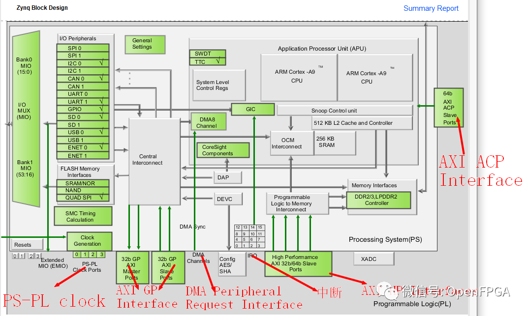
The Zynq PS and PL are interconnected through the following interfaces:
- Two 32-bit master AXI ports (PS master)
- Two 32-bit slave AXI ports (PL master)
- Four 32/64-bit slave high-performance ports (PL master)
- One 64-bit slave Accelerator Coherency Port (ACP) (PL master)
- Four clocks from PS to PL
- Interrupts from PS to PL
- Interrupts from PL to PS
- DMA peripheral request interface
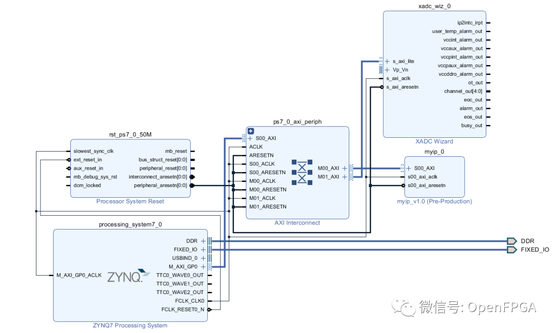
The following is a block diagram illustrating these different interface points:
ARM’s AXI is a burst-oriented protocol designed to provide high bandwidth while maintaining low latency. Each AXI port contains independent read and write channels. A version of the AXI protocol used for less demanding interfaces is AXI4-Lite, which is a simpler protocol suitable for register control/status interfaces. For example, the Zynq XADC connects to the Zynq PS using the AXI4-Lite interface. For more information on the AXI protocol, please visit:
http://www.arm.com/products/system-ip/amba/amba-open-specifications.php
The Zynq SoC supports three different AXI transfer types that can be used to connect the PS to the PL devices:
- AXI4 Burst transfers
- AXI4-Lite for simple control interfaces
- AXI4-Streaming for unidirectional data transfers
The following table defines the theoretical bandwidth for each interface:
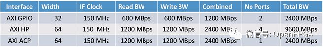
To achieve the maximum speeds listed in the table above, the DMA controller of the Zynq SoC must be used. As an additional benefit, when the PS is the master, the DMA controller reduces the load on the ARM Cortex-A9 MPCore processor of the Zynq SoC. Without using the DMA controller, the maximum transfer rate from the PS to the PL is 25 Mbytes/sec.
In summary, an astonishing theoretical bandwidth of 14.4 Gbytes/sec (115.2 Gbits/sec) is utilized between the PS and PL!
Creating AXI Peripherals
This section will create a peripheral in the programmable logic structure of the Zynq SoC using the AXI interface.
Step One
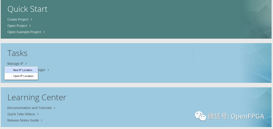
The first step is to open the Vivado design and select the “Create and Package IP” option from the tools menu.
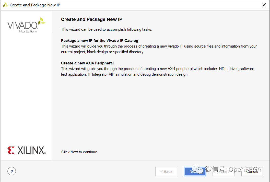
This will open a dialog that allows the creation of an AXI4 peripheral. The first actual page of the dialog provides many options for creating new IP or converting the current design or directory into an IP module.
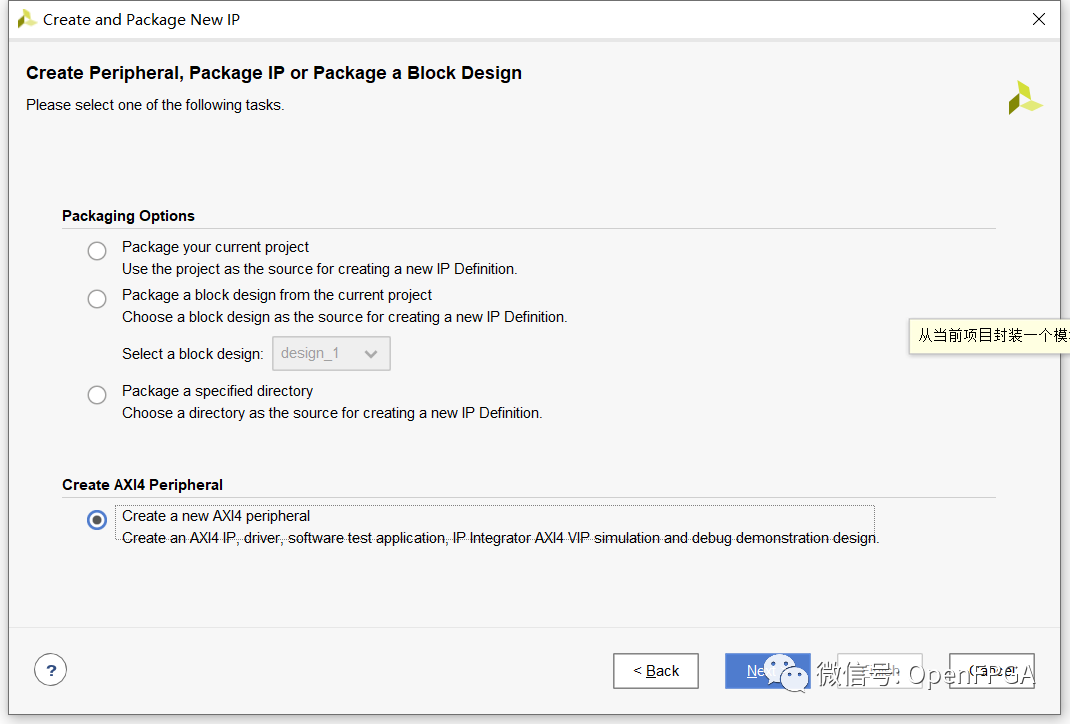
Select the “Create new AXI4 peripheral” option and point it to a predefined IP location. A new IP location can be created using the IP management section on the Vivado home page.
Then, the dialog allows you to enter the library, name, description, and company URL to be used for the new peripheral. For this very simple example (which I will expand on later).
The next dialog is a powerful dialog where we can define the AXI4 interface types we wish to specify:
- Master or Slave
- Interface type – Lite, Streaming, or Burst
- Bus width 32 or 64 bits
- Memory size
- Number of registers
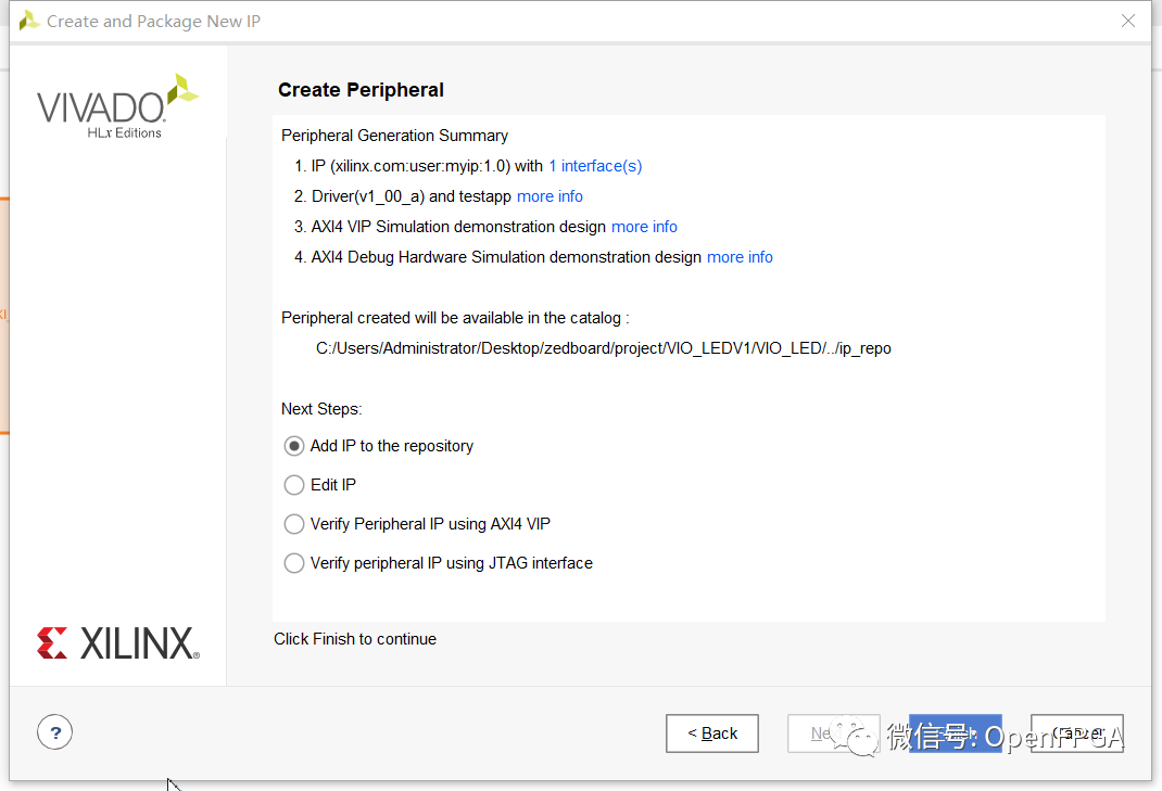
This initial example is very simple so that I can demonstrate the process required to create a peripheral, implement it in Vivado, and then export it to the SDK. For this reason, I will only have an AXI4-Lite interface with four registers, which we can address using software. These registers can be used to control the functional operations of the programmable logic aspect of the design.

The final “Create Peripheral” dialog allows you to select an option to generate driver files for the new peripheral. This is an important step as it will make the peripheral easier to use with the SDK.
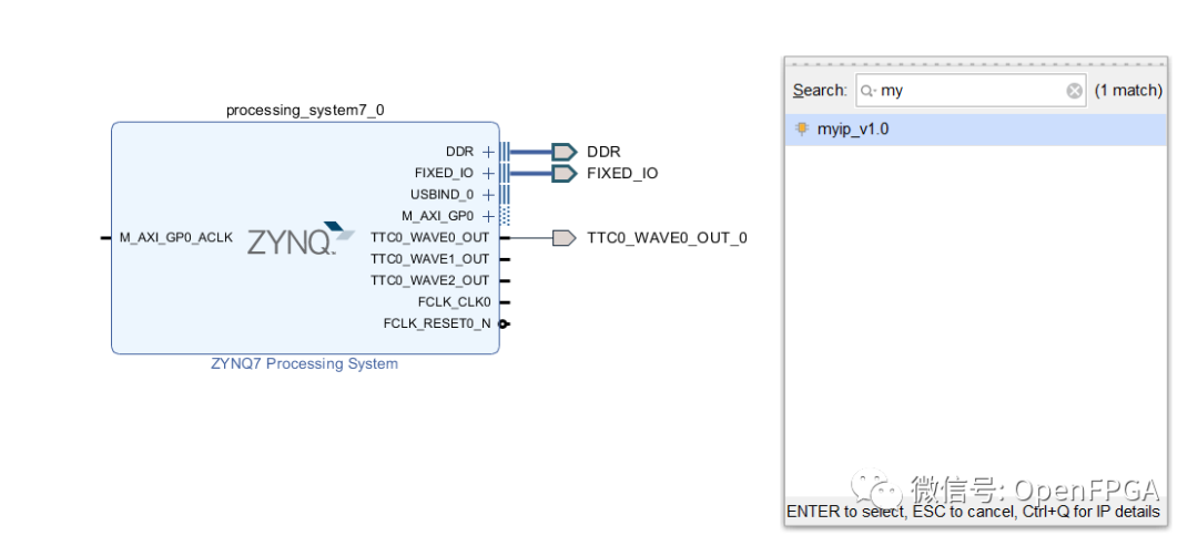
Once the “Create Peripheral” wizard is closed, you can open the created VHDL file and add custom hardware design to perform the desired functionality in the PL. I will only use the four registers we created, so I can leave the file unedited. After creating the peripheral, we want to connect and use it in the Vivado design. This is very simple. We open the system block diagram and select the add IP option from the left menu. The peripheral created should be found in this menu. Available peripherals are listed alphabetically.
Step Two
Drag this IP module into the design and connect it to the AXI GP bus, where Vivado provides a run connection automation tool.
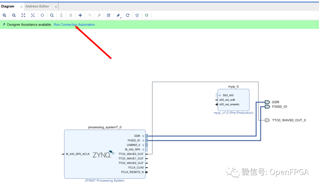
Running the tool will produce a design that we can implement.
The address range of the peripheral can be modified by clicking on the address editor tab. Note that a 4k address space is the minimum allowed address space, which is overly generous for our four register example. Fortunately, the ARM Cortex-A9 MPCore processor in the Zynq SoC has a large address space.
Once Vivado has automatically completed the connections and address space allocation, as shown in the figure below, we can implement the design and export it to the SDK. Then we can start using our peripheral.
Note that the implementation report can be checked to ensure the created peripheral is included.
Verification
We have generated an AXI peripheral above, and the next step is to verify the correctness of this peripheral in the SDK.
Use Vivado to create the AXI4 peripheral and generate the BIN file.
After creating the hardware components of the design, we now need to export it to our SDK design so that we can write software to drive it. The first step is to open the current project in Vivado, compile to generate the BIN file, and then export the hardware to the SDK. (If you try to export hardware while the SDK is in use, you will receive a warning.) If the hardware is not exported to the SDK, the next time you open the SDK, you will need to update the hardware definition and board support package, or you will not be able to use them. You will also need to update the repository defined in the design to include the IP repository containing the peripheral.
Open the xparameters.h file (in the BSP include files) to view the address space dedicated to the new AXI4 peripheral:
The next step is to open the System.MSS file and customize the BSP to use the driver generated during the peripheral creation process instead of the generic driver.

Rebuilding the project ensures that the driver files are loaded into the BSP. This is a very useful step as these files also contain a simple self-test program that can be used to test whether the software interface of the peripheral is correct before starting to use it for more advanced operations. Using this test program also indicates that we have correctly instantiated the hardware in Vivado.
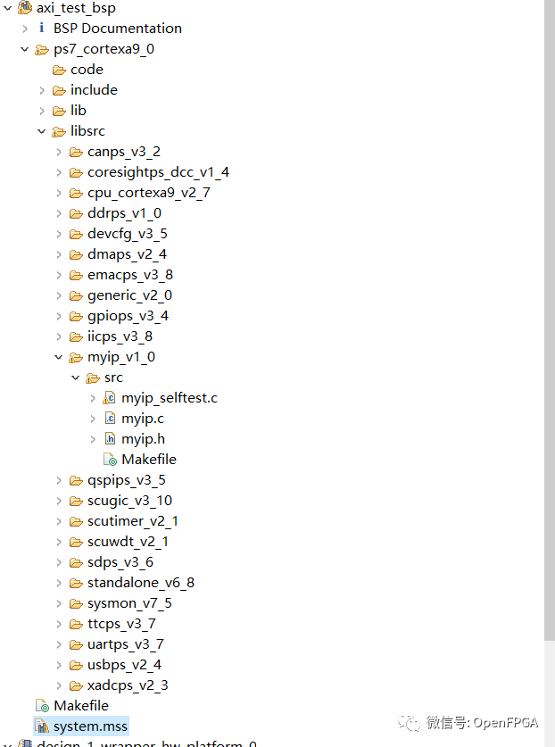
Under the BSP libsrc, you will see many files for the new AXI4 peripheral. These files allow reading and writing to the peripheral just like using native peripherals (such as XADC and GPIO) that we have been using in other articles.
For this simple example, the file myip.h contains three functions we can use to drive the new peripheral.
-
MYIP_mReadReg(BaseAddress, RegOffset)
-
MYIP_mWriteReg(BaseAddress, RegOffset, Data)
-
XStatus MYIP_Reg_SelfTest(void * baseaddr_p);
Aside from the self-test function, the read and write functions map to the generic functions Xil_In32 and Xil_Out32, which are defined in Xil_io.h. However, using the created functions can make the code more readable as the addressed peripheral is very clear.
For this example, we only have four registers in the peripheral, so we will only use the self-test, which will write to and read from all registers and report pass or fail. This test gives us confidence that we have the correct hardware and software environment, and once we define them in the peripheral module, we can proceed to use more advanced functionalities. In the next article, we will explore how to add some functionality to the peripheral using HDL code to offload functions from the processing system and improve system performance.
Using XADC for Complex Calculations
Suppose we want to perform more complex calculations in Zynq, such as for industrial control systems. Typically, these systems will have multiple analog inputs (via ADC) driven by thermistors, thermocouples, pressure sensors, platinum resistance thermometers (PRT), and other sensors.
Often, data from these sensors requires transfer functions to convert raw data values from the ADC into data suitable for further processing. A good example is the Zynq XADC, which includes many functions/macros in XADCPS.h for converting raw XADC values into voltage or temperature. However, these conversions are very simple. If these calculations become more complex, the processing time required by Zynq increases. If the programmable logic (PL) side of the Zynq SoC is used to perform these calculations, the computation speed can be significantly accelerated. An added benefit is that the processor can free up time to perform other software tasks, thus improving processing bandwidth by using PL for calculations.
The more complex the transfer function, the more processor time is required for the calculation results. We can use the example of converting atmospheric pressure in millibars to height in meters to demonstrate this conversion. The following transfer function gives the altitude for pressure between 0 and 10 millibars:
Implementing this transfer function using the processing system (PS) of the Zynq SoC is straightforward, using the following line of code where “result” is a float; a, b, and c are constants defined in the transfer function above; and i is the input value:
result = ((float)a*(i*i)) + ((float)b*(i)) + (float)c;
For this example, I will use code nested in a “for” loop to simulate the steps in the input values above. The code outputs the result via STDOUT. Since I want to calculate the time required to execute this calculation, I will use a private timer to determine this time, as follows:
for(i=0.0; i<10.0; i = i +0.1 ){
       XScuTimer_LoadTimer(&Timer, TIMER_LOAD_VALUE);
       timer_start = XScuTimer_GetCounterValue(&Timer);
       XScuTimer_Start(&Timer);
       result = ((float)a*(i*i)) + ((float)b*(i)) + (float)c;
       XScuTimer_Stop(&Timer);
       timer_value = XScuTimer_GetCounterValue(&Timer);
      printf("%f,%f,%lu,%lu, \n\r",i,result,timer_start, timer_value);
     }
While this code may not provide the most accurate timing reference, it is sufficient to demonstrate the principles we are studying. Running the above code on the Zynq board yielded the following results in the terminal window. Note:

A simple analysis of this output indicates that the calculation results require an average of 25 CPU_3x2x clock cycles. With a 666MHz processor clock, this calculation takes 76 ns. I believe many will see that the ADC output is not a floating point but a fixed point. Rewriting the function code using integer math resulted in a very similar average number of clock cycles. However, I think for this example, floating point is easier to use and does not require explaining the principles behind the fixed-point system.
After determining how long it takes for the PS side of Zynq to execute a moderately complex transfer function, next time we can see how fast we can compute this function when we move the same function to the PL side of the device.
How Fixed-Point Numbers Work
In the previous section, we used the PS to calculate a formula, and next, we will use the PL side to accelerate this formula calculation. However, the PL side is characterized by only being able to perform fixed-point calculations, so this section will explain how fixed-point numbers work.
There are two ways to represent numbers in digital systems: fixed-point or floating-point. Fixed-point representation keeps the decimal point in a fixed position, which greatly simplifies arithmetic operations. As shown, a fixed-point number consists of two parts called the integer and fractional parts: the integer part of the number is to the left of the implied decimal point, and the fractional part is to the right.
The above fixed-point number can represent unsigned numbers between 0.0 and 255.9906375 or signed numbers between -128.9906375 and 127.9906375 using two’s complement representation.
Floating-point numbers are divided into two parts: the exponent and the mantissa. Floating-point representation allows the decimal point to float within the number based on the size of the value. The main disadvantage of fixed-point representation is that to represent larger numbers or achieve more accurate results using decimals, more bits are required. While FPGAs can support both fixed-point and floating-point numbers simultaneously, most applications adopt fixed-point systems because they are easier to implement than floating-point systems.
In designs, we can choose to use either unsigned or signed numbers. Typically, the choice is constrained by the algorithm being implemented. Unsigned numbers can represent a range from 0 to 2^n – 1 and always represent positive numbers. Signed numbers use the two’s complement number system to represent both positive and negative numbers. The two’s complement system allows one number to be subtracted from another simply by adding the two numbers. The range of values that can be represented by two’s complement numbers is: – (2^n-1) ~ + (2^n-1 – 1)
The normal way to represent the split between integer and fractional bits in fixed-point numbers is x,y, where x represents the number of integer bits and y represents the number of fractional bits. For example, 8,8 represents 8 integer bits and 8 fractional bits, while 16,0 represents 16 integer bits and 0 fractional bits.
In many cases, the number of integer and fractional bits will be determined at design time, typically after the algorithm has been converted from floating-point. Due to the flexibility of FPGAs, we can represent fixed-point numbers of arbitrary bit lengths; we are not limited to 32, 64, or even 128-bit registers. FPGAs are equally applicable to 15-bit, 37-bit, or 1024-bit registers.
The number of integer bits required depends on the maximum integer value that needs to be stored. The number of fractional bits depends on the desired precision of the final result. To determine the required number of integer bits, we can use the following equation:
For example, the number of integer bits required to represent values between 0.0 and 423.0 is:
We need 9 integer bits, allowing representation of a range from 0 to 511.
Two fixed-point operands must have their decimal points aligned to add, subtract, or divide the two numbers. That is, an x,8 number can only be added to, subtracted from, or divided by another number in the same x,8 representation. To perform arithmetic operations on numbers of different x,y formats, we must first align the decimal points. Note that aligning the decimal points for division is not strictly necessary. However, implementing fixed-point division requires careful consideration to ensure the correct results in such cases.
Similarly, when multiplying two fixed-point numbers, the decimal points do not need to be aligned. For example, multiplying two fixed-point numbers formatted as 14,2 and 10,6 results in 24,8 (formatted as 24 integer bits and 8 fractional bits). For division by a fixed constant, we can simplify the design by calculating the reciprocal of the constant and then using that constant result as a multiplier.
Accelerating PS Calculations with PL
The previous section briefly discussed the basics of implementing fixed-point calculations in the PL side, and now we will focus on implementing PL-side acceleration in the system.
Before we start cutting the code, we need to determine the scaling factor (the position of the decimal point) we will use in this specific implementation. In this example, the input signal ranges from 0 to 10, so we can pack 4 decimal places and 12 fractional places into a 16-bit input vector.
The formula above is what we want to implement, which has three constants A, B, and C: A = -0.0088 B = 1.7673 C = 131.29. We need to handle (scale) these constants in the implementation. The benefit of doing this in the FPGA is that we can scale each constant differently to optimize performance, as shown in the table below:
When implementing the above equation, we need to consider the synthesis vector expansion for the terms Ax^2 and Bx defined as follows:
To perform the final addition with constant C, we need to align the decimal points. Therefore, we need to divide the results and Ax^2 and Bx by a power of 2 to align the decimal point with C. The result will also be formatted to this value, i.e., 8,8.
After calculating the above, we are ready to implement the design in the Vivado peripheral project we created in the previous sections.
The first implementation step is to open the block diagram view in Vivado, right-click on the IP, and select “Edit in IP Packager”. Once the IP Packager opens in the top-level file, we can easily implement a simple process that performs calculations over multiple clock cycles. (In this example, five clocks, although it can be further optimized.)
Now we can repackage and rebuild the project in Vivado before exporting the updated hardware to the SDK (remember to update the version number).
In the SDK, we can use the same method as before, except now we use the fixed-point number system instead of the floating-point system used in the previous example:
  for(i=0; i<2560; i = i+25 ){
       XScuTimer_LoadTimer(&Timer, TIMER_LOAD_VALUE);
       timer_start = XScuTimer_GetCounterValue(&Timer);
       XScuTimer_Start(&Timer);
       ADAMS_PERIHPERAL_mWriteReg(Adam_Low, 4, i);
       result = ADAMS_PERIHPERAL_mReadReg(Adam_Low, 12);
       XScuTimer_Stop(&Timer);
       timer_value = XScuTimer_GetCounterValue(&Timer);
      printf("%d,%lu,%lu,%lu, \n\r",i,result,timer_start, timer_value);
     }
When the above code runs on the ZYNQ board, we see the following output results on the serial port:
The result of 33610 equals 131.289 divided by 2^8, which is correct and matches the floating-point calculation. Although the numerical results are the same, the biggest difference is the time required to execute the calculations. While the actual computation of the peripheral design only requires 5 clocks, generating the result takes 140 clocks or 420ns, while using the ARM Cortex-A9 processor on the PS side of the Zynq SoC takes 25 CPU clocks.
Why is there a difference? Shouldn’t the PL side be faster? The main reason is the overhead of peripheral I/O time. When using the PL side, we must consider the bus latency on the AXI bus and the AXI bus frequency, which in this application is 142.8MHz (requesting 150MHz). The AXI bus overhead causes the computation time to be longer than expected. However, nothing is wrong. The mistake is in the direction I took: because of this I/O overhead time, moving tasks to the PL of the Zynq SoC is not used in this way.
So what should we do to take a more reasonable approach? DMA
In the next article, we will use DMA to transport data and see if the results are what we want~~
Some source files for this article:
https://gitee.com/openfpga/zynq-chronicles/blob/master/VHDL_part24.vhd
ZYNQ: From Abandonment to Entry (Part 1) – MIO

ZYNQ: From Abandonment to Entry (Part 2) – PS GPIO

ZYNQ: From Abandonment to Entry (Part 3) – Interrupts (Part 1)
ZYNQ: From Abandonment to Entry (Part 4) – Interrupts (Part 2)

ZYNQ: From Abandonment to Entry (Part 5) – Dedicated Timers
ZYNQ: From Abandonment to Entry (Part 6) – Dedicated Watchdog