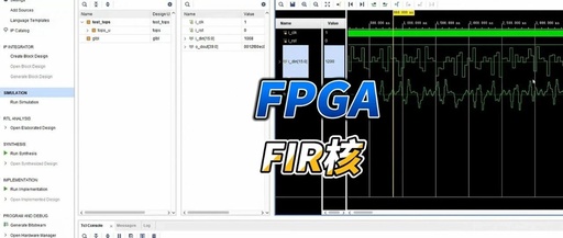
FPGA Hardware Development – Clock Analysis

FPGA Hardware Development - Clock Analysis

FPGA Clock Analysis The clock system is the “heart” of FPGA design, and its performance directly determines the system’s timing margin, operating frequency, and stability. Effective clock analysis can help engineers identify timing bottlenecks, optimize clock architecture, and ensure reliable operation of the design at the target frequency. This article will systematically analyze the composition, … Read more

A Step-by-Step Guide to Utilizing the MIPI Interface on Zhi Duo Jing FPGA: A Game Changer for Video Project Development!

A Step-by-Step Guide to Utilizing the MIPI Interface on Zhi Duo Jing FPGA: A Game Changer for Video Project Development!

Hello everyone! Today, we are going to discuss a very practical topic—how to use the MIPI interface on Zhi Duo Jing FPGA. Whether it’s for camera image acquisition or display control, MIPI is a very common interface standard. Mastering it will greatly enhance your video project development efficiency! The Zhi Duo Jing FPGA supports the … Read more

Texas Instruments Launches Stackable DC/DC Buck Converter for Enhanced Power Density in High-Current FPGAs and Processors

Texas Instruments Launches Stackable DC/DC Buck Converter for Enhanced Power Density in High-Current FPGAs and Processors

Texas Instruments (TI) today launched a new stackable integrated circuit (IC) 40-A SWIFT™ DC/DC buck converter. The TPS546D24A PMBus buck converter can deliver up to 160A of output current at an ambient temperature of 85°C, which is four times higher than other power integrated circuits on the market. Among many 40A DC/DC converters, the TPS546D24A … Read more

Xilinx Unveils Software-Programmable Chip Design for Data Centers: Introducing the Adaptive Compute Acceleration Platform

Xilinx Unveils Software-Programmable Chip Design for Data Centers: Introducing the Adaptive Compute Acceleration Platform

According to ZDNet Source: ZDNet Semiconductor company Xilinx has recently unveiled its software-programmable chip design for data centers, which Xilinx claims is part of a new category of computing. The software-programmable chip design for data centers is named the Adaptive Compute Acceleration Platform (ACAP). Xilinx states that ACAP will make highly programmable data center servers … Read more

Exclusive Interview with Xilinx Director: When CPUs Encounter Performance ‘Ceilings’

Exclusive Interview with Xilinx Director: When CPUs Encounter Performance 'Ceilings'

In 2014, Lenovo’s acquisition of IBM’s x86 server business and Motorola Mobility’s smartphone business attracted widespread attention in the industry. However, note that the acquisition amounts were only $2.3 billion and $2.9 billion, respectively. At the end of last year, a merger involving $16.7 billion did not receive much attention domestically. In fact, the acquirer … Read more

PCIe Bus: The High-Speed Data Engine in Communication and Networking

PCIe Bus: The High-Speed Data Engine in Communication and Networking

1. Core Advantages of PCIe Technology: Why is it the Cornerstone of Communication Networks? PCIe[Peripheral Component Interconnect Express] is a high-speed serial point-to-point dual-channel bus standard, whose technical characteristics perfectly meet the high bandwidth and low latency requirements of modern communication networks: 1. Full-duplex communication architecture allows each device to have independent transmit (TX) and … Read more

The Rise of RISC-V: SiFive Launches Five New RISC-V Cores

The Rise of RISC-V: SiFive Launches Five New RISC-V Cores

👋 Hello, this is 「V Da Lang」, focusing on RISC-V industry information, technology trends, and development resources. Remember to follow me.. 01 — SiFive Launches Five New RISC-V Cores, Accelerating the New Wave of AI Workloads SiFive announced the release of its second-generation Intelligence™ series in September 2025, which includes five new or upgraded versions … Read more

Design and Implementation of SoC IP Verification Scheme Based on ZYNQ

Design and Implementation of SoC IP Verification Scheme Based on ZYNQ

Authors:Tao Qingping, Shang Guoqing, Zhu QingAffiliation:1. China Electronics Technology Group Corporation, the 58th Research Institute, Wuxi, Jiangsu 214035.Abstract:With the popularity of SoC chip design, the demand for various IP designs is also increasing. The challenge for IC design engineers and verification engineers is how to quickly and accurately verify the correctness of these IP functions. … Read more

Detailed Explanation of Binary Operations (Addition, Subtraction, Multiplication, Division) in FPGA

Detailed Explanation of Binary Operations (Addition, Subtraction, Multiplication, Division) in FPGA

In FPGA design, binary operations are one of the most fundamental and commonly used logical operations, with addition, subtraction, multiplication, and division widely applied in digital signal processing, control algorithms, and data computation scenarios. To simplify hardware implementation while accommodating signed operations, FPGAs typically use two’s complement representation for signed numbers. Using two’s complement not … Read more

FPGA Tutorial Case 5: ROM Design and Implementation Based on Vivado Core

FPGA Tutorial Case 5: ROM Design and Implementation Based on Vivado Core

01ROM Design and Implementation Based on Vivado Core In FPGAs, ROM is a very important module that allows complex data to be output based on address information. Vivado is a high-level design suite from Xilinx used for the design and verification of FPGAs (Field Programmable Gate Arrays). In Vivado, we can use high-level design methods … Read more