Skip to content
This article is excerpted from “2022 Research Framework for Domestic Server CPUs“. In the post-Moore’s Law era, the performance benefits brought by the improvement of process technology are already very limited. The Dennard Scaling law constraints have led to a sharp increase in chip power consumption, and the cost of transistors has risen instead of falling; single-core performance has approached its limit, and the performance improvement of multi-core architectures is also slowing down. With the arrival of the AIoT era, the downstream demand for computing power is showing diversification and fragmentation, making it difficult for general-purpose processors to cope.
1) From General Purpose to Specialized: Chips customized for different scene characteristics have emerged, including XPU, FPGA, DSA, and ASIC.
2) From Bottom Layer to Top Layer: Software, algorithms, and hardware architecture. Optimizing architecture can greatly enhance processor performance. For example, AMD’s Zen3 merged two separate 16MB L3 Caches into one 32MB L3 Cache, and with improved branch prediction and wider floating-point units, it increased single-core performance by 19% compared to Zen2.
3) Heterogeneous and Integrated: The launch of Apple’s M1 Ultra chip brings enlightenment, utilizing gradually maturing technologies such as 3D packaging and inter-chip interconnect to effectively integrate multiple chips, which seems to be the best way to continue Moore’s Law.
Mainstream chip manufacturers have begun comprehensive layouts: Intel now has CPU, FPGA, and IPU product lines, increasing investment in GPU product lines and launching the latest Falcon Shores architecture to refine heterogeneous packaging technology; Nvidia has successively released multi-chip module (MCM) Grace series products, which are expected to enter mass production soon; AMD recently completed the acquisition of Xilinx, and is expected to move towards CPU+FPGA heterogeneous integration in the future.
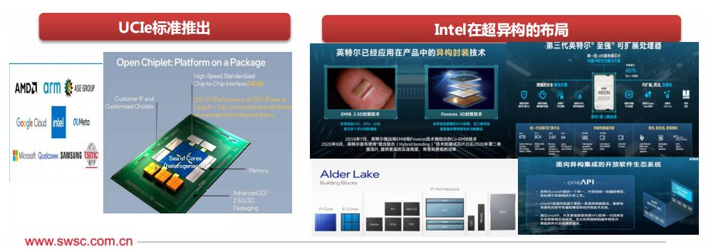
In addition, major industry participants including Intel, AMD, Arm, Qualcomm, TSMC, Samsung, ASE, Google Cloud, Meta, and Microsoft have jointly established the Chiplet Standard Alliance, officially launching the high-speed interconnect standard for general Chiplets, “Universal Chiplet Interconnect Express” (UCIe).
Under the UCIe framework, the interconnect interface standards are unified. Various Chiplet chips with different processes and functions are expected to be integrated through various packaging methods such as 2D, 2.5D, and 3D, forming a large-scale complex chip system with multiple processing engines, which has the advantages of high bandwidth, low latency, and economic energy savings.
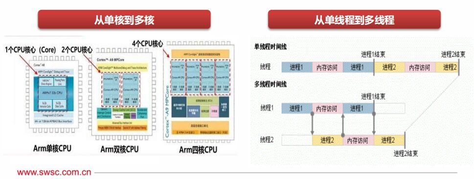
Enhancing performance-power ratio through multi-core: Multi-core processors integrate multiple processing cores onto the same chip, significantly increasing the computational performance density of each unit. At the same time, the existing peripheral components can be shared by multiple CPU systems, leading to higher communication bandwidth and shorter communication delays. Multi-core processors have a natural advantage in parallelism and can effectively reduce power consumption and enhance performance through dynamic voltage/frequency adjustments and load optimization.
Improving overall performance through multi-threading: By replicating the structural state on the processor, multiple threads on the same processor can execute synchronously and share the processor’s execution resources, achieving a significant increase in overall performance and throughput at a minimal hardware cost.
Microarchitecture improvements
A large number of arithmetic units, logic units, and registers are interconnected through tri-state buses and unidirectional buses, forming the CPU microarchitecture. Different microarchitecture designs play an intuitively important role in enhancing CPU performance and efficiency.
Upgrading the microarchitecture generally involves a series of complex tasks such as instruction set expansion, hardware virtualization, large memory, and out-of-order execution, and also requires modifications at the software level, including compilers and function libraries, affecting the entire system.
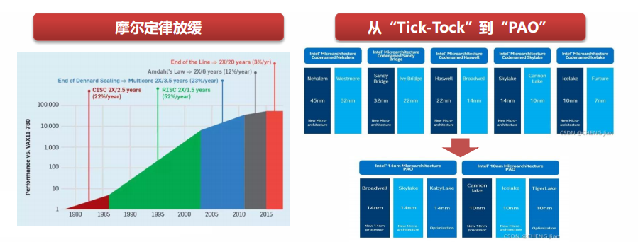
Moore’s Law was proposed in the 1960s, and until 2011, the miniaturization of computer components was the main factor in improving processing performance. After 2011, Moore’s Law began to slow down, and improvements in silicon processing technology no longer provide significant performance boosts.
Failure of the “Tick-Tock” model
Since 2007, Intel has implemented the “Tick-Tock” development model, with a two-year cycle, launching new process technology in odd years (Tick) and new microprocessor architectures in even years (Tock).
After the continuous delays from 14nm to 10nm, Intel announced in 2016 the cessation of the “Tick-Tock” processor upgrade cycle, shifting to a three-step strategy for processor upgrades: process technology (Process) – architecture update (Architecture) – optimization (Optimization).
In the post-Moore era, top-level optimization may be more important.
New bottom-layer optimization paths have been proposed, such as 3D stacking, quantum computing, photonics, superconducting circuits, and graphene chips, which are still in their infancy but are expected to break existing imagination in the future.
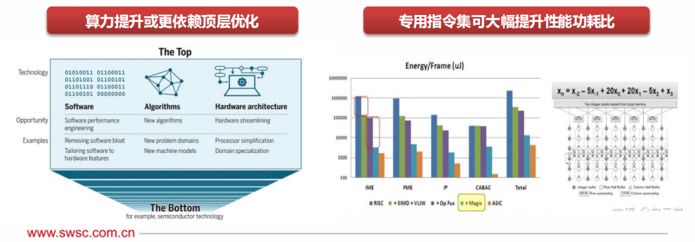
According to an article published by MIT in Science, in the post-Moore’s Law era, improvements in computing power will increasingly come from the “top level” of the computing stack, namely software, algorithms, and hardware architecture.
General-purpose instruction sets often need to support thousands of instructions to cover more applications, leading to a very complex design for the pipeline front end (fetching, decoding, branch prediction, etc.), which negatively impacts performance and power consumption.
Domain-specific instruction sets can greatly reduce the number of instructions, increase operational granularity, and integrate memory access optimization, achieving an order of magnitude improvement in performance-power ratio.
Emergence of new scenarios, CPU development from general to specialized.
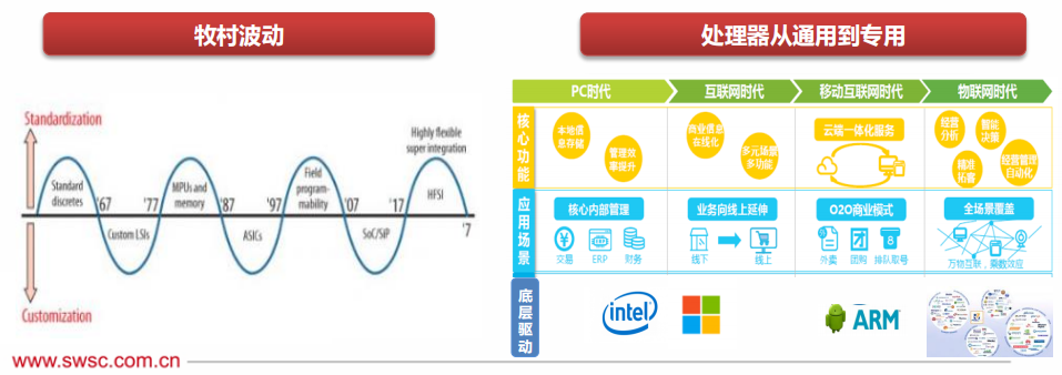
In 1972, Gordon Bell proposed that every ten years, a new type of computer (new programming platform, new network connection, new user interface, new usage methods, and cheaper) would emerge, forming a new industry. In 1987, former Hitachi chief engineer Tsugio Makimoto proposed that semiconductor products may progress along the alternating paths of “standardization” and “customization,” fluctuating approximately every ten years.
After the desktop PC, internet era, and mobile internet era, “Internet of Everything” has become a new trend, and AIoT is triggering the third wave of revolution in the global information industry. The most obvious feature of AIoT is the fragmentation of demand, making existing general-purpose processor design methods difficult to effectively meet customized needs.
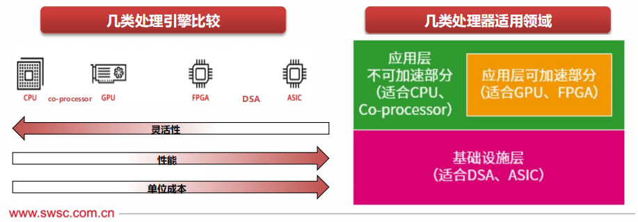
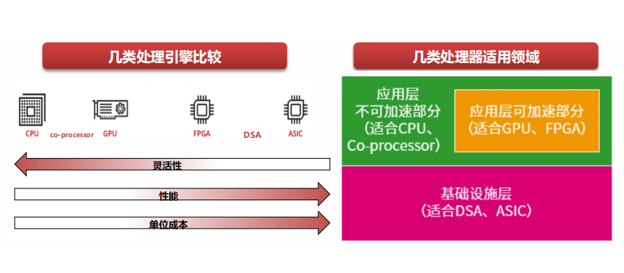
General-purpose and performance are hard to achieve simultaneously.
CPU is the most general-purpose processing engine, with the most basic instructions and the best flexibility.Coprocessors are engines based on CPU extended instruction sets, such as ARM’s NEON, Intel’s AVX, AMX extended instruction sets, and corresponding coprocessors.
GPU, in essence, is a parallel processing of many small CPU cores, thus NP, Graphcore’s IPU, and others are at the same level of processing type as GPUs.
FPGA, architecturally, can be used to implement customized ASIC engines, but due to its hardware programmability, it can switch to other ASIC engines, providing a certain degree of flexible programmability.
DSA is close to ASIC design but has a certain degree of programmability. It covers a broader range of fields and scenarios than ASIC, but there are still too many areas that require specific DSA to cover.
ASIC is a fully non-programmable custom processing engine, theoretically capable of the most complex “instructions” and the highest performance efficiency. Because the covered scenarios are very small, a large number of ASIC processing engines are needed to cover various scenarios.
In the post-Moore’s Law era, looking ahead to the future development path of CPUs.
Irreversible SoC integration: Due to the continuous increase in integration of integrated circuits, integrating all different functional blocks of a complete computer onto a single chip has become a trend in the entire semiconductor industry, significantly reducing system costs and power consumption while improving system reliability. The M1 is not a CPU in the traditional sense, but a SoC. The CPU consists of 8 cores, including 4 high-performance cores and 4 high-efficiency cores. Each high-performance core provides excellent single-thread task processing performance while minimizing power consumption within allowable limits.
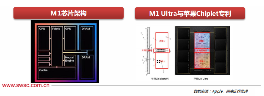 Significant enhancement of heterogeneous capabilities: The M1 also adopts a unified memory architecture (UMA), with the CPU, GPU, neural engine, cache, and DRAM memory all connected through a high-speed Fabric bus. Thanks to this, all modules in the SoC can access the same data without needing to copy data between multiple memory pools, resulting in higher bandwidth and lower latency, greatly improving processor performance and power efficiency. Additionally, the latest generation M1 Ultra is essentially an effective combination of two M1 MAX chips, providing up to 128G unified memory and achieving an 8-fold increase in GPU performance compared to M1.
The Apple M1 processor has completed a transition from multi-chip to integration, which is also a necessary step for Apple to build a complete PC ecosystem, revealing more possibilities for the future development of CPUs.
In the post-Moore era, heterogeneity and integration.
Overseas chip giants are actively laying out heterogeneous computing: Intel has now laid out CPU, FPGA, IPU, and GPU product lines, and has successively announced new architectures such as Alder Lake and Falcon Shores; Nvidia has successively released multi-chip module (MCM, Multi-Chip Module) Grace series products, which are expected to enter mass production soon; AMD recently completed the acquisition of Xilinx, and is expected to move towards CPU+FPGA heterogeneous integration in the future.
Significant enhancement of heterogeneous capabilities: The M1 also adopts a unified memory architecture (UMA), with the CPU, GPU, neural engine, cache, and DRAM memory all connected through a high-speed Fabric bus. Thanks to this, all modules in the SoC can access the same data without needing to copy data between multiple memory pools, resulting in higher bandwidth and lower latency, greatly improving processor performance and power efficiency. Additionally, the latest generation M1 Ultra is essentially an effective combination of two M1 MAX chips, providing up to 128G unified memory and achieving an 8-fold increase in GPU performance compared to M1.
The Apple M1 processor has completed a transition from multi-chip to integration, which is also a necessary step for Apple to build a complete PC ecosystem, revealing more possibilities for the future development of CPUs.
In the post-Moore era, heterogeneity and integration.
Overseas chip giants are actively laying out heterogeneous computing: Intel has now laid out CPU, FPGA, IPU, and GPU product lines, and has successively announced new architectures such as Alder Lake and Falcon Shores; Nvidia has successively released multi-chip module (MCM, Multi-Chip Module) Grace series products, which are expected to enter mass production soon; AMD recently completed the acquisition of Xilinx, and is expected to move towards CPU+FPGA heterogeneous integration in the future.
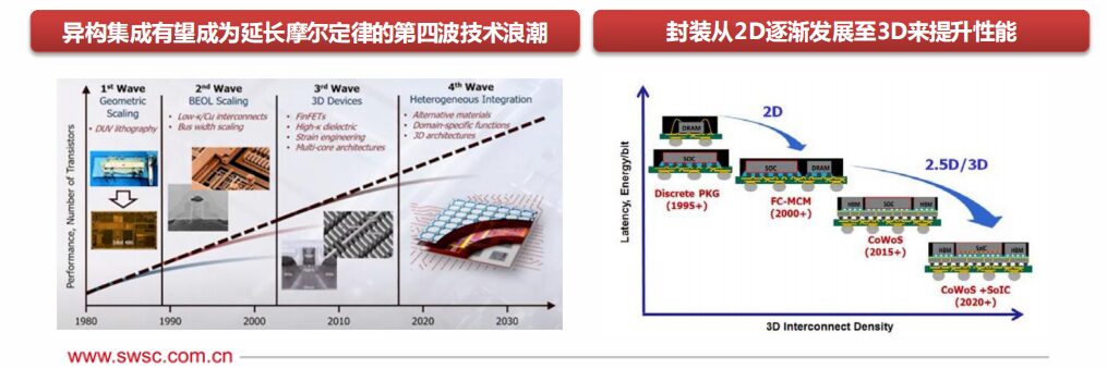 Wafer fabs and packaging plants are also actively investing in heterogeneous integration: Heterogeneous computing requires advanced integrated packaging technology. The development of advanced packaging and chip stacking technologies in the past decade, such as 3D stacking and SiP, has made heterogeneous integration significantly possible. Currently, 2.5D packaging technology has developed relatively maturely, such as TSMC’s CoWoS, Samsung’s I-Cube, and 3D packaging has become a focus for major wafer fabs. Intel has begun mass production of Foveros technology, Samsung has completed the verification of X-Cube, and TSMC has also proposed the SoiC integration solution.
CPU+XPU is widely used, but there is still room for optimization. Traditional heterogeneous computing architectures have inherent problems such as long IO paths and resource loss in input and output, and still cannot fully balance extreme performance and flexibility.
The Chiplet alliance is formed to explore super heterogeneous possibilities. On March 3, 2022, Intel, AMD, Arm, Qualcomm, TSMC, Samsung, ASE, Google Cloud, Meta, Microsoft, and other ten industry giants jointly established the Chiplet Standard Alliance, officially launching the high-speed interconnect standard for general Chiplets, “Universal Chiplet Interconnect Express” (UCIe).
Under the UCIe framework, the interconnect interface standards are unified. Various Chiplet chips with different processes and functions are expected to be integrated through various packaging methods such as 2D, 2.5D, and 3D, forming a large-scale complex chip system with multiple processing engines, which has the advantages of high bandwidth, low latency, and economic energy savings.
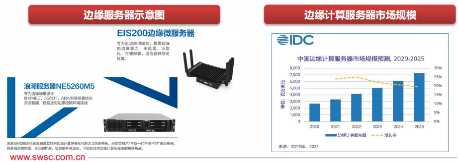
Edge computing servers are essential products to solve the “computing power shortage” in the AIoT era.
Cloud computing cannot meet the massive and real-time processing demands. With the gradual maturity of technologies such as artificial intelligence, 5G, and the Internet of Things, the demand for computing power is extending from data centers to the edge to generate faster network service responses, meeting the basic needs of industries in real-time business, application intelligence, security, and privacy protection.
Explosive growth in market size. According to IDC, the overall market size of edge computing servers in China reached $3.31 billion, growing by 23.9% compared to 2020, with a projected CAGR of 22.2% from 2020 to 2025, higher than the global average of 20.2%.
Rapid increase in customized servers. Currently, general-purpose servers and edge customized servers account for 87.1% and 12.9%, respectively. As edge application scenarios gradually diversify, there will be a rapid increase in demand for edge customized servers with specific form factors, low energy consumption, wider operating temperatures, and other specific designs. IDC predicts that edge customized servers will maintain a compound growth rate of 76.7%, with a penetration rate exceeding 40% by 2025.
Integrated solutions customized according to diverse business scenarios are a trend.
Unlike data center servers, edge servers do not solely pursue the highest computing performance, maximum storage, or maximum expansion card counts, but rather aim to provide flexible configurations within limited space. Currently, edge servers are mainly used in industrial manufacturing and other fields, requiring the selection of motherboards, processors, etc., based on specific environments (high pressure, low temperature, extreme weather), with downstream demand showing fragmentation and no unified standards.
As more and more computing and storage demands are pushed to the edge, the current trend typically involves tighter acceleration integration, to meet various needs, including AI computing power. Hyperscale cloud providers are beginning to study classification architectures to reduce the fragmentation inevitably caused by familiar multi-tenant methods, where computing, storage, networking, and memory become a set of combinable structures, with rack-style architectures (RSA) deploying CPU, GPU, hardware acceleration, RAM, storage, and networking capacity separately.
Cloud servers are replacing traditional servers globally.
The development of cloud servers has made China a major global server power. With the development and application of new generation information technologies such as mobile terminals and cloud computing, enterprises and governments are gradually migrating their businesses from traditional data centers to cloud data centers. Although the current cloud computing market in China is relatively behind that of the United States, recent years have seen China’s cloud computing development speed significantly surpass the global cloud computing market growth rate, and this trend is expected to continue in the future.
Wafer fabs and packaging plants are also actively investing in heterogeneous integration: Heterogeneous computing requires advanced integrated packaging technology. The development of advanced packaging and chip stacking technologies in the past decade, such as 3D stacking and SiP, has made heterogeneous integration significantly possible. Currently, 2.5D packaging technology has developed relatively maturely, such as TSMC’s CoWoS, Samsung’s I-Cube, and 3D packaging has become a focus for major wafer fabs. Intel has begun mass production of Foveros technology, Samsung has completed the verification of X-Cube, and TSMC has also proposed the SoiC integration solution.
CPU+XPU is widely used, but there is still room for optimization. Traditional heterogeneous computing architectures have inherent problems such as long IO paths and resource loss in input and output, and still cannot fully balance extreme performance and flexibility.
The Chiplet alliance is formed to explore super heterogeneous possibilities. On March 3, 2022, Intel, AMD, Arm, Qualcomm, TSMC, Samsung, ASE, Google Cloud, Meta, Microsoft, and other ten industry giants jointly established the Chiplet Standard Alliance, officially launching the high-speed interconnect standard for general Chiplets, “Universal Chiplet Interconnect Express” (UCIe).
Under the UCIe framework, the interconnect interface standards are unified. Various Chiplet chips with different processes and functions are expected to be integrated through various packaging methods such as 2D, 2.5D, and 3D, forming a large-scale complex chip system with multiple processing engines, which has the advantages of high bandwidth, low latency, and economic energy savings.
Edge computing servers are essential products to solve the “computing power shortage” in the AIoT era.
Cloud computing cannot meet the massive and real-time processing demands. With the gradual maturity of technologies such as artificial intelligence, 5G, and the Internet of Things, the demand for computing power is extending from data centers to the edge to generate faster network service responses, meeting the basic needs of industries in real-time business, application intelligence, security, and privacy protection.
Explosive growth in market size. According to IDC, the overall market size of edge computing servers in China reached $3.31 billion, growing by 23.9% compared to 2020, with a projected CAGR of 22.2% from 2020 to 2025, higher than the global average of 20.2%.
Rapid increase in customized servers. Currently, general-purpose servers and edge customized servers account for 87.1% and 12.9%, respectively. As edge application scenarios gradually diversify, there will be a rapid increase in demand for edge customized servers with specific form factors, low energy consumption, wider operating temperatures, and other specific designs. IDC predicts that edge customized servers will maintain a compound growth rate of 76.7%, with a penetration rate exceeding 40% by 2025.
Integrated solutions customized according to diverse business scenarios are a trend.
Unlike data center servers, edge servers do not solely pursue the highest computing performance, maximum storage, or maximum expansion card counts, but rather aim to provide flexible configurations within limited space. Currently, edge servers are mainly used in industrial manufacturing and other fields, requiring the selection of motherboards, processors, etc., based on specific environments (high pressure, low temperature, extreme weather), with downstream demand showing fragmentation and no unified standards.
As more and more computing and storage demands are pushed to the edge, the current trend typically involves tighter acceleration integration, to meet various needs, including AI computing power. Hyperscale cloud providers are beginning to study classification architectures to reduce the fragmentation inevitably caused by familiar multi-tenant methods, where computing, storage, networking, and memory become a set of combinable structures, with rack-style architectures (RSA) deploying CPU, GPU, hardware acceleration, RAM, storage, and networking capacity separately.
Cloud servers are replacing traditional servers globally.
The development of cloud servers has made China a major global server power. With the development and application of new generation information technologies such as mobile terminals and cloud computing, enterprises and governments are gradually migrating their businesses from traditional data centers to cloud data centers. Although the current cloud computing market in China is relatively behind that of the United States, recent years have seen China’s cloud computing development speed significantly surpass the global cloud computing market growth rate, and this trend is expected to continue in the future.
 Providing diverse computing power for different needs. Generally, small websites with less data request processing usually use 1 or 2-core CPUs; local portals and small industry websites require CPUs with more than 4 cores; while e-commerce platforms and video websites require CPUs with more than 16 cores. In addition, cloud servers also provide flexible expansion and upgrade services, generally supporting the loading of heterogeneous computing power.
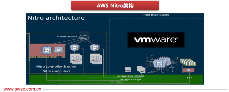
CPU+ASIC, the heterogeneous trend of cloud servers is obvious.
In traditional computer virtualization architectures, the business layer is virtual machines, and the management layer is the host machine, with business and management coexisting on the CPU, resulting in only about 70% of CPU resources being available to users.
AWS creatively restructured the architecture, separating business and management into two hardware entities, with business running on the CPU and management on the NITRO chip, thus moving virtualization losses to a custom Nitro system and improving security.
The Nitro architecture is not only powerful but also particularly flexible, capable of running virtual machines based on common hypervisors (such as qemu-kvm, vmware) and even running operating systems directly, saving 30% of CPU resources.
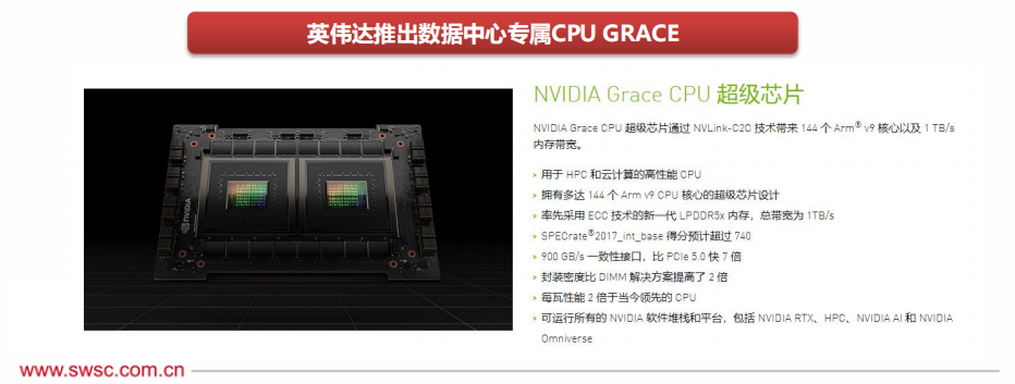
ARM may become an important challenger, as Nvidia launches the first CPU dedicated to data centers, GRACE.
The public cloud giants are fiercely competing on prices, and strict energy consumption control in first-tier cities in China makes ARM’s advantages in mobile terminals and low energy consumption characteristics an important solution for large data centers to address energy-saving and cost issues. Under the background of domestic self-control trends, if a strong ecological alliance can be built, it would be the most powerful challenger to potentially disrupt the existing pattern in the future.
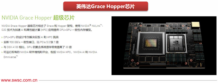
Nvidia announced the launch of its first CPU dedicated to AI infrastructure and high-performance computing, the Nvidia Grace, which consists of two CPU chips interconnected by the latest generation NVLink-C2C technology.
Grace is based on the latest ARMv9 architecture, with 144 CPU cores per socket, utilizing error-correcting codes (ECC) and other mechanisms to provide twice the memory bandwidth and energy efficiency of today’s leading server chips, with outstanding compatibility, capable of running all of Nvidia’s software stacks and platforms, including Nvidia RTX, HPC, Omniverse, etc.
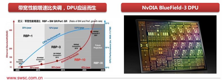
DPU, or Data Processing Unit, primarily serves as an offloading engine for the CPU, mainly processing network and IO data, providing bandwidth compression, security encryption, network function virtualization, and other functions to free up CPU computing power for higher-level applications.
In 2013, AWS developed Nitro and Alibaba Cloud developed X-Dragon, both of which can be seen as precursors to DPU; Nvidia officially released a product named “DPU” in 2020, defining it as the third main chip after CPU and GPU, marking another milestone in heterogeneous computing.
DPU is a good complement to CPU and GPU. According to Nvidia’s prediction, every server may not have a GPU, but must have a DPU, with the number of DPUs in data centers expected to reach the same level as data center servers.
AI models are trained through hundreds of billions of parameters, enhancing deep recommendation systems that contain trillions of bytes of data, and their complexity and scale are experiencing explosive growth. These massive models are challenging the limits of current systems, and optimizing solely with CPU is insufficient to meet their performance demands.
Therefore, AI servers mainly adopt heterogeneous forms, typically in rack form. In heterogeneous configurations, they can combine CPU with GPU, CPU with FPGA, CPU with TPU, CPU with ASIC, or CPU with multiple accelerator cards.
Currently, AI servers on the market generally adopt the CPU+GPU configuration, as GPUs differ from CPUs in that they use a parallel computing model, excelling at handling intensive data operations, such as graphics rendering and machine learning. To continue expanding models for high accuracy and practicality, there is a need for rapid access to large memory pools and tight coupling between CPU and GPU.
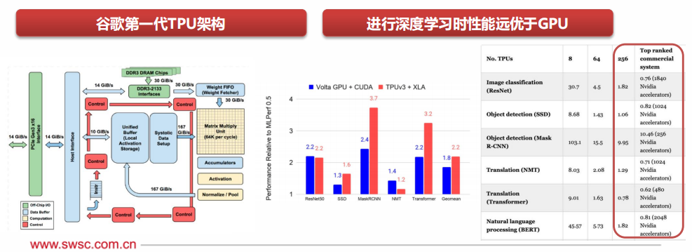
TPU, or Tensor Processing Unit, is a dedicated integrated circuit (DSA) developed by Google to accelerate deep learning, using a custom CISC instruction set, modified logic, circuits, arithmetic units, memory system architecture, and on-chip interconnect, optimized for frameworks such as TensorFlow.
Starting in 2015, Google released TPUv1 for specific internal projects such as Alpha Go; in 2018, Google released TPUv3 and began selling it to third parties, marking the gradual commercialization of TPU.
In 2021, Google released TPUv4i, which improved performance by 2.7 times compared to the third generation TPU; 256 TPU chips completed the famous “BERT” model training in the NLP field in just 1.82 minutes, while under the same conditions, using Nvidia A100 GPU took 3.36 minutes.
Welcome angel round andAround companies to join the group (Friendly connections with 500 automotive investment institutions, including top organizations; several companies have been completed);There are communication groups for leaders of science and technology innovation companies and groups related to the automotive industry, automotive semiconductors, key components, new energy vehicles, intelligent connected vehicles, aftermarket, automotive investment, autonomous driving, vehicle networking, etc. For group entry, please scan the administrator’s WeChat (Please indicate your company name)
Providing diverse computing power for different needs. Generally, small websites with less data request processing usually use 1 or 2-core CPUs; local portals and small industry websites require CPUs with more than 4 cores; while e-commerce platforms and video websites require CPUs with more than 16 cores. In addition, cloud servers also provide flexible expansion and upgrade services, generally supporting the loading of heterogeneous computing power.
CPU+ASIC, the heterogeneous trend of cloud servers is obvious.
In traditional computer virtualization architectures, the business layer is virtual machines, and the management layer is the host machine, with business and management coexisting on the CPU, resulting in only about 70% of CPU resources being available to users.
AWS creatively restructured the architecture, separating business and management into two hardware entities, with business running on the CPU and management on the NITRO chip, thus moving virtualization losses to a custom Nitro system and improving security.
The Nitro architecture is not only powerful but also particularly flexible, capable of running virtual machines based on common hypervisors (such as qemu-kvm, vmware) and even running operating systems directly, saving 30% of CPU resources.
ARM may become an important challenger, as Nvidia launches the first CPU dedicated to data centers, GRACE.
The public cloud giants are fiercely competing on prices, and strict energy consumption control in first-tier cities in China makes ARM’s advantages in mobile terminals and low energy consumption characteristics an important solution for large data centers to address energy-saving and cost issues. Under the background of domestic self-control trends, if a strong ecological alliance can be built, it would be the most powerful challenger to potentially disrupt the existing pattern in the future.
Nvidia announced the launch of its first CPU dedicated to AI infrastructure and high-performance computing, the Nvidia Grace, which consists of two CPU chips interconnected by the latest generation NVLink-C2C technology.
Grace is based on the latest ARMv9 architecture, with 144 CPU cores per socket, utilizing error-correcting codes (ECC) and other mechanisms to provide twice the memory bandwidth and energy efficiency of today’s leading server chips, with outstanding compatibility, capable of running all of Nvidia’s software stacks and platforms, including Nvidia RTX, HPC, Omniverse, etc.
DPU, or Data Processing Unit, primarily serves as an offloading engine for the CPU, mainly processing network and IO data, providing bandwidth compression, security encryption, network function virtualization, and other functions to free up CPU computing power for higher-level applications.
In 2013, AWS developed Nitro and Alibaba Cloud developed X-Dragon, both of which can be seen as precursors to DPU; Nvidia officially released a product named “DPU” in 2020, defining it as the third main chip after CPU and GPU, marking another milestone in heterogeneous computing.
DPU is a good complement to CPU and GPU. According to Nvidia’s prediction, every server may not have a GPU, but must have a DPU, with the number of DPUs in data centers expected to reach the same level as data center servers.
AI models are trained through hundreds of billions of parameters, enhancing deep recommendation systems that contain trillions of bytes of data, and their complexity and scale are experiencing explosive growth. These massive models are challenging the limits of current systems, and optimizing solely with CPU is insufficient to meet their performance demands.
Therefore, AI servers mainly adopt heterogeneous forms, typically in rack form. In heterogeneous configurations, they can combine CPU with GPU, CPU with FPGA, CPU with TPU, CPU with ASIC, or CPU with multiple accelerator cards.
Currently, AI servers on the market generally adopt the CPU+GPU configuration, as GPUs differ from CPUs in that they use a parallel computing model, excelling at handling intensive data operations, such as graphics rendering and machine learning. To continue expanding models for high accuracy and practicality, there is a need for rapid access to large memory pools and tight coupling between CPU and GPU.
TPU, or Tensor Processing Unit, is a dedicated integrated circuit (DSA) developed by Google to accelerate deep learning, using a custom CISC instruction set, modified logic, circuits, arithmetic units, memory system architecture, and on-chip interconnect, optimized for frameworks such as TensorFlow.
Starting in 2015, Google released TPUv1 for specific internal projects such as Alpha Go; in 2018, Google released TPUv3 and began selling it to third parties, marking the gradual commercialization of TPU.
In 2021, Google released TPUv4i, which improved performance by 2.7 times compared to the third generation TPU; 256 TPU chips completed the famous “BERT” model training in the NLP field in just 1.82 minutes, while under the same conditions, using Nvidia A100 GPU took 3.36 minutes.
Welcome angel round andAround companies to join the group (Friendly connections with 500 automotive investment institutions, including top organizations; several companies have been completed);There are communication groups for leaders of science and technology innovation companies and groups related to the automotive industry, automotive semiconductors, key components, new energy vehicles, intelligent connected vehicles, aftermarket, automotive investment, autonomous driving, vehicle networking, etc. For group entry, please scan the administrator’s WeChat (Please indicate your company name)