Chip packaging, simply put, is the process of placing the integrated circuit die produced by the foundry onto a substrate that serves as a carrier, then bringing out the pins and securing the package into a whole. It protects the chip, acting as its shell, not only fixing and sealing the chip but also enhancing its electrical and thermal performance. Therefore, packaging is very important for CPUs and other LSI integrated circuits.
The types of packaging can generally be divided into DIP Dual In-line Package and SMD Surface Mount Device.
From a structural perspective, packaging has evolved from the early transistor TO (such as TO-89, TO-92) packaging to dual in-line packaging, followed by the development of SOP (Small Outline Package) by PHILIP, which has gradually derived into SOJ (J-type small outline package), TSOP (Thin Small Outline Package), VSOP (Very Small Outline Package), SSOP (Shrink SOP), TSSOP (Thin Shrink SOP), SOT (Small Outline Transistor), and SOIC (Small Outline Integrated Circuit).
In terms of material medium, it includes metals, ceramics, and plastics. Many circuits that require high-strength working conditions, such as military and aerospace levels, still use a lot of metal packaging.
The following are the mainstream packaging types compiled by the editor:

1. DIP Dual In-line Package
DIP refers to integrated circuit chips packaged in a dual in-line form. Most medium and small scale integrated circuits (ICs) use this packaging format, with pin counts generally not exceeding 100. ICs using DIP packaging have two rows of pins that need to be inserted into a chip socket with a DIP structure. Of course, they can also be directly soldered onto a circuit board with the same number of solder holes and geometric arrangement. Care should be taken when inserting and removing DIP packaged chips from sockets to avoid damaging the pins.
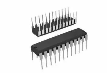
DIP Packaging Diagram
DIP packaging has the following characteristics:
1. Suitable for through-hole soldering on PCB (Printed Circuit Board), easy to operate.
2. The ratio of chip area to package area is relatively large, thus the volume is also larger.
DIP is the most popular insert-type package, used in standard logic ICs, memory, and microelectronic circuits, etc.
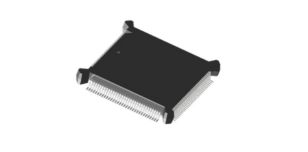
2. QFP/PFP Type Package
QFP/PFP packaged chips have very small distances between pins, and the pins are thin. Generally, large-scale or ultra-large scale integrated circuits adopt this packaging form. Chips packaged in this way must use SMD (Surface Mount Device) technology to solder the chip to the main board.
With SMD installation, chips do not need to have holes drilled in the main board; corresponding solder points are designed on the surface of the main board. Aligning the chip pins with the corresponding solder points allows for soldering to the main board.
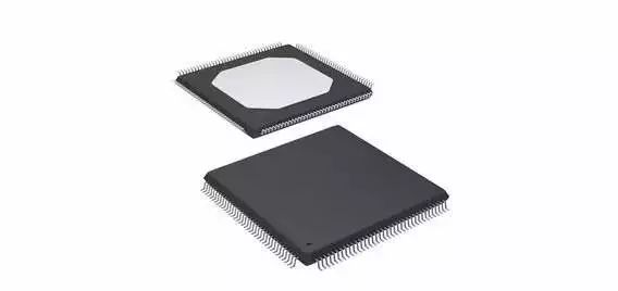
QFP Packaging Diagram
QFP/PFP packaging has the following characteristics:
1. Suitable for SMD surface mounting technology on PCB circuit boards.
2. Low cost, suitable for medium to low power, ideal for high-frequency applications.
3. Easy to operate, high reliability.
4. The ratio of chip area to package area is relatively small.
5. A mature packaging type that can adopt traditional processing methods.
Currently, QFP/PFP packaging is widely used, with many MCU manufacturers’ A chips adopting this package.
3. BGA Type Package
As integrated circuit technology has developed, the requirements for IC packaging have become stricter. This is because packaging technology relates to the functionality of the product. When the frequency of an IC exceeds 100MHZ, traditional packaging methods may produce the so-called “CrossTalk” phenomenon, and when the number of pins exceeds 208, traditional packaging methods become challenging.
Therefore, in addition to using QFP packaging, most high-pin-count chips now use BGA (Ball Grid Array Package) packaging technology.
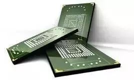
BGA Packaging Diagram
BGA packaging has the following characteristics:
1. Although the number of I/O pins increases, the distance between pins is much greater than in QFP packaging, improving yield.
2. The contact area of BGA solder balls with the substrate is large and short, which is beneficial for heat dissipation.
3. The short pins of BGA solder balls shorten the signal transmission path, reducing lead inductance and resistance; signal transmission delay is small, and the frequency adaptability is greatly improved, thus enhancing circuit performance.
4. Assembly can use coplanar soldering, greatly improving reliability.
5. BGA is suitable for MCM packaging, enabling high density and high performance in MCM.
4. SOP Package
SOP (Small Outline Package) is one of the surface mount packaging types, with pins extending from both sides of the package in a seagull wing shape (L shape). It can be made of plastic or ceramic. Later, SOP derived into SOJ (J-type pin small outline package), TSOP (Thin Small Outline Package), VSOP (Very Small Outline Package), SSOP (Shrink SOP), TSSOP (Thin Shrink SOP), SOT (Small Outline Transistor), and SOIC (Small Outline Integrated Circuit).
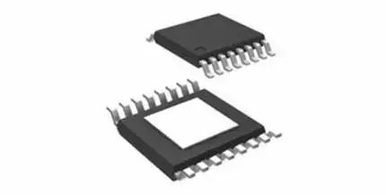
SOP Packaging Diagram
The typical feature of this type of packaging is that many pins are made around the packaged chip, making the packaging operation easy and reliable, and it is currently one of the mainstream packaging methods, truly a system-level package. It is commonly used in some types of memory ICs.
Several Chip Packages Derived from SOP:
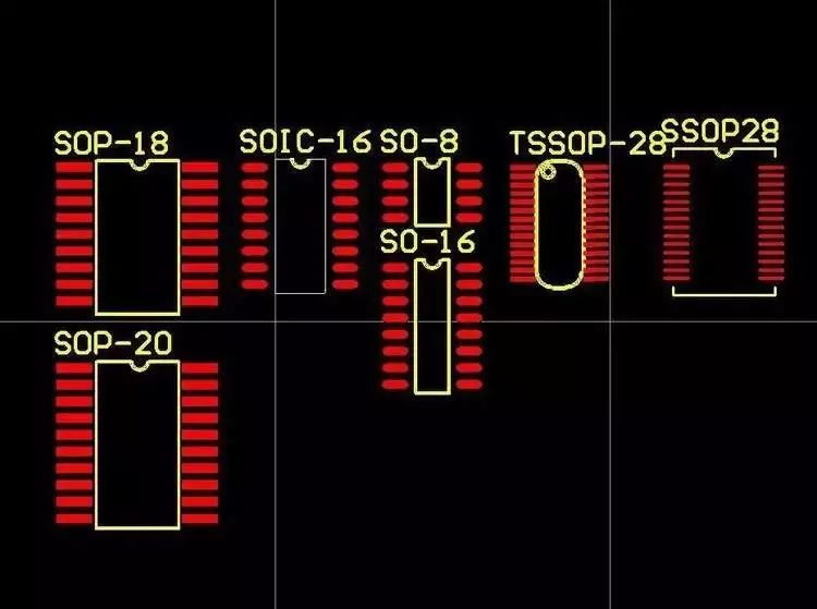
Comparison of SOP/SOIC/TSSOP/SSOP Packaging Diagrams
SOIC
SOIC (Small Outline Integrated Circuit Package) is derived from SOP, with the specific dimensions of the two packages being essentially the same, including the length, width, pin width, and pin spacing of the chip. Therefore, in PCB design, SOP and SOIC can be mixed.
SOIC is a surface mount integrated circuit package form that reduces space by about 30-50% compared to an equivalent DIP package, and reduces thickness by about 70%. The corresponding DIP package has the same pin leads. The naming convention for this type of packaging is to add the number of pins after SOIC or SO. For example, a 14-pin 4011 package would be named SOIC-14 or SO-14.
TSOP
TSOP stands for Thin Small Outline Package. A typical feature of TSOP memory packaging technology is the arrangement of pins around the packaged chip. TSOP is suitable for SMT (Surface Mount Technology) installation on PCB (Printed Circuit Board). The parasitic parameters (voltage disturbances caused by large current changes) are reduced in TSOP packaging dimensions, making it suitable for high-frequency applications, easy to operate, and highly reliable.
5. QFN Package
QFN is a leadless quad flat package, featuring a chip pad for mechanical and thermal integrity exposure with peripheral terminal pads.
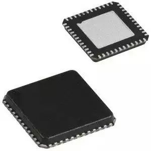
QFN Packaging Diagram
This package can be square or rectangular. Electrodes are configured on all four sides of the package. Due to the leadless design, the mounting area is smaller than that of QFP, and the height is lower than that of QFP.
Characteristics of QFN Packaging:
1. Surface mount packaging, leadless design;
2. Lead pad design occupies less PCB area;
3. Extremely thin components (<1mm), suitable for applications with strict space requirements;
4. Very low impedance and self-inductance, suitable for high-speed or microwave applications;
5. Excellent thermal performance, mainly due to the large area of the heat dissipation pad at the bottom;
6. Lightweight, suitable for portable applications.
The small form factor of QFN packaging can be used in laptops, digital cameras, personal digital assistants (PDAs), mobile phones, and MP3 players, among other portable consumer electronics. From a market perspective, QFN packaging is increasingly gaining attention from users. Considering cost and volume factors, QFN packaging is expected to be a growth point in the coming years, with very optimistic development prospects.
6. PLCC Package
PLCC is a plastic chip packaging carrier with leads. It is a surface mount type of package, with pins extending from all four sides of the package in a T-shape, and its dimensions are much smaller than DIP packaging. PLCC packaging is suitable for SMT surface mounting technology on PCBs, with the advantages of small size and high reliability.
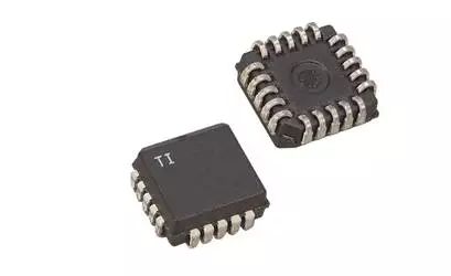
PLCC Packaging Diagram
PLCC is a special lead chip package, which is a surface mount package where the leads bend inward at the bottom of the chip, making them invisible from the top view. The soldering of this type of chip uses a reflow soldering process, requiring specialized soldering equipment, and it is quite troublesome to remove the chip during debugging, so it is rarely used now.
Due to the diversity of IC packaging types, it does not significantly affect R&D testing, but for mass production in factories, the more types of IC packaging, the more corresponding programming socket models need to be selected. ZLG Electronics has been specializing in the chip programming industry for more than a decade, and its programmers support and provide various packaging type IC programming sockets for factory mass production.
7. PQFP Package
PQFP stands for Plastic Quad Flat Package. The distance between the pins of PQFP packaged chips is very small, and the pins are thin. Generally, large-scale or ultra-large scale integrated circuits adopt this packaging form, with pin counts generally over 100.
PQFP Packaging Diagram
8. CSP Chip Size Package
With the increasing demand for personalization and compactness in global electronic products, packaging technology has progressed to CSP (Chip Size Package). It reduces the size of the chip package to match the size of the bare chip, meaning the packaged IC size is no more than 1.2 times the size of the chip, and the IC area is no more than 1.4 times that of the die.
CSP packaging can be divided into four types:
1. Lead Frame Type (traditional lead frame type), with representative manufacturers including Fujitsu, Hitachi, Rohm, and Goldstar.
2. Rigid Interposer Type, with representatives including Motorola, Sony, Toshiba, and Panasonic.
3. Flexible Interposer Type, with the most famous being Tessera’s microBGA and CTS’s sim-BGA using the same principle. Other representative manufacturers include General Electric (GE) and NEC.
4. Wafer Level Package (WLP): Unlike traditional single chip packaging methods, WLCSP cuts the entire wafer into individual chips, which is touted as the future mainstream of packaging technology. Companies that have invested in R&D include FCT, Aptos, Casio, EPIC, Fujitsu, and Mitsubishi Electric.
CSP packaging is suitable for ICs with fewer pins, such as memory modules and portable electronic products. In the future, it will be widely used in information appliances (IA), digital televisions (DTV), e-books, wireless networks WLAN/Gigabit Ethernet, ADSL/mobile phone chips, Bluetooth, and other emerging products.
9. CLCC Package
CLCC is a ceramic chip carrier with leads, one of the surface mount packaging types, with pins extending from all four sides of the package in a T-shape. It is used for packaging UV-erasable EPROMs and MEMS circuits with EPROMs. This package is also referred to as QFJ or QFJ-G.
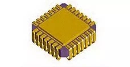
CLCC Packaging Diagram
10. Flip Chip Package
Flip Chip, also known as flip chip, is one of the more mainstream packaging forms in recent years, mainly used in high-end devices and high-density packaging fields. Among all surface mounting technologies, flip chip can achieve the smallest and thinnest packaging.
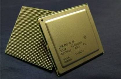
IBM Flip Chip Packaging Diagram
Compared to COB, this packaging form has its chip structure and I/O ends (solder balls) facing down. Since the I/O leads are distributed across the entire chip surface, flip chip has reached its peak in packaging density and processing speed. In particular, it can use techniques similar to SMT for processing, making it the ultimate direction in chip packaging technology and high-density installation.

▲ TO Transistor Outline Package
TO (Transistor Outline) refers to the early packaging specifications, such as TO-92, TO-92L, TO-220, TO-252, etc., which are all insert-type packaging designs. In recent years, the demand for surface mount packaging has increased, and TO packages have also progressed to surface mount packaging.
▲ PGA Pin Grid Array Package
PGA (Pin Grid Array Package) chip packaging form has multiple square arrays of pins both inside and outside the chip, with each square array of pins arranged around the chip at specific intervals. Depending on the number of pins, it can form 2-5 circles. During installation, the chip is inserted into a dedicated PGA socket.
▲ MCM Multi-Chip Model
There was once a thought: when single-chip integration could not yet reach the level of multiple chips, could high-integration, high-performance, and high-reliability CSP chips (using LSI or IC) and dedicated integrated circuit chips (ASIC) be assembled into various electronic components, subsystems, or systems on high-density multi-layer interconnect substrates using surface mount technology (SMT)? This idea gave rise to multi-chip modules (MCM). It will have a significant impact on modern computing, automation, and communication industries.
▲ Cerdip
Cerdip is a glass-sealed ceramic dual in-line package used for ECL RAM, DSP (Digital Signal Processor), and other circuits. Cerdip with a glass window is used for UV-erasable EPROMs and MEMS circuits with built-in EPROM. The pin center distance is 2.54mm, and the number of pins ranges from 8 to 42. In Japan, this package is referred to as DIP-G (where G means glass sealed).
▲ LGA (Land Grid Array)
LGA is a contact array packaging type, which has an array of flat electrode contacts on the bottom surface of the package. During assembly, it is simply inserted into a socket. Currently, practical ceramic LGA with 227 contacts (1.27mm center distance) and 447 contacts (2.54mm center distance) is used in high-speed logic LSI circuits. Compared to QFP, LGA can accommodate more input/output pins in a smaller package. Additionally, due to the low resistance of the leads, it is very suitable for high-speed LSI. However, due to the complexity of socket manufacturing and high costs, it is now rarely used.
▲ QFI (Quad Flat I-leaded Package)
QFI is a flat package with I-shaped leads on all four sides. It is one of the surface mount packaging types. The leads extend from the four sides of the package and point downwards in an I shape. It is also referred to as MSP. The mounting is connected by bump soldering to the printed circuit board. Since the leads do not protrude, the mounting area is smaller than that of QFP. Hitachi developed and used this package for video analog ICs. Additionally, Motorola’s PLL ICs in Japan also use this packaging.
▲ SIP Single In-line Package
European semiconductor manufacturers often use the name SIL (Single In-line). The leads extend from one side of the package, arranged in a straight line. When assembled onto a printed circuit board, the package stands upright. The lead center distance is usually 2.54mm, with the number of pins ranging from 2 to 23, mostly custom products. The shapes of the packages vary. Some packages with shapes similar to ZIP are also referred to as SIP.
▲ TCP
Thin film packaging TCP technology is mainly used in Intel Mobile Pentium MMX. CPUs using TCP packaging technology generate significantly less heat compared to ordinary PGA pin array CPUs at the time, allowing for smaller additional cooling devices and improving the space utilization of the main unit, thus commonly seen in ultra-thin laptops. However, since TCP packaging involves directly soldering the CPU to the motherboard, ordinary users cannot replace it.
▲ SIMM Single In-line Memory Module
A memory module with electrodes located near one side of the printed circuit board, typically referring to components inserted into sockets. The standard SIMM has two specifications: 30 electrodes with a center distance of 2.54mm and 72 electrodes with a center distance of 1.27mm. SIMMs using SOJ packaging with 1 Mbit and 4 Mbit DRAM have been widely used in personal computers, workstations, and other devices. At least 30-40% of DRAM is assembled in SIMMs.
▲ DIMM (Dual Inline Memory Module)
The dual in-line memory module is quite similar to SIMM, except that the gold fingers at both ends of DIMM are not interconnected like SIMM; they each independently transmit signals, thus meeting the transmission needs of more data signals.
Disclaimer: Content is sourced from the internet and exclusively compiled by Mantech. Please indicate the source when reprinting.

Previous Recommendations
iPhone 8 Material Exposure, Component Price Increase Causes Cost Surge! (Including the Most Comprehensive Apple Supply Chain)
It’s All About Housing Prices: Shenzhen Dongguan Factories Frequently Shut Down, What Kind of House Can Lang Ping, Who Earns 7 Million a Year, Buy?
Despair, Regret, Confusion: The New Generation of Huawei Employees Overwhelmed by High Housing Prices
The Top 50 EMS Companies Globally Generated $270 Billion Last Year!
Summary of Core Suppliers in the Electronics Industry Chain (Updated Regularly)
Chinese Money is Being Earned by These American Semiconductor Companies!
The 35 Most Profitable Connector Manufacturers are All Here (Including Agent List)
Drone Supply Chain Overview (Including 13 Major Control Chip Manufacturers)
Winning First Place: Shenzhen’s Top 30 IC Design Companies Are All Here!
Breaking News! China’s Counterfeit Components Have Been Seized Again in Europe

Hunting Chip’s Second Anniversary, 100,000 Cash Red Packets Are Given Out Nonstop, Click “Read Original” Now!