1. Definition
A PCB buried via is a hole that connects different layers of conductive traces within a multilayer printed circuit board. Unlike through holes and blind vias, buried vias are completely hidden inside the PCB and are not visible on the surface. This design allows the PCB to maintain high-density routing while optimizing signal transmission paths and reducing electromagnetic interference (EMI).
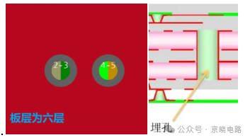 2.Applicable Scenarios01High-Density PCB Design
In complex circuits that require high-density routing, buried via technology plays a crucial role. It effectively saves surface space on the circuit board, allowing for a more compact layout and higher component integration; it also significantly improves routing flexibility, optimizing signal transmission paths and enhancing overall circuit performance and stability.
02High-Speed Signal Transmission
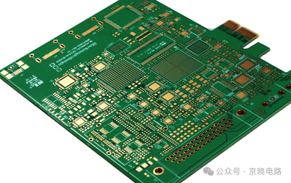
In high-speed digital circuits or radio frequency (RF) circuits, buried vias can reduce signal path lengths, lowering signal loss and delay. In multilayer PCB designs, buried vias can optimize inter-layer connections and reduce the impact of through holes on signal integrity.
03Space-Constrained Devices
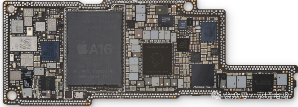
In miniaturized electronic products such as smartphones, tablets, and wearable devices, buried via technology is crucial as it helps achieve a more compact design layout while ensuring high-performance signal transmission.
3.Advantages of Buried Vias01Space Saving, Enhanced Design Flexibility
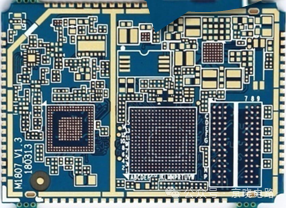
Buried vias do not occupy surface space on the PCB, allowing the surface to be used for placing more components or routing, enabling designers to freely route between internal layers and optimize circuit layouts.
02Improved Signal Integrity, Reduced Electromagnetic Interference
Buried via technology effectively reduces signal reflection and crosstalk by shortening signal transmission paths, significantly enhancing the overall performance of the circuit. Additionally, this technology reduces the length and number of surface traces, effectively lowering electromagnetic radiation and interference levels.
03Aesthetics
Since buried vias are hidden within the PCB and do not occupy surface space, this makes the surface design of the PCB cleaner and smoother, resulting in a more elegant visual effect. This characteristic makes PCBs using buried via technology particularly suitable for products with high aesthetic design requirements.
4.Conclusion
PCB buried vias, as an advanced circuit board design technology, play an important role in high-density interconnections, high-speed signal transmission, and miniaturized devices. By saving space, improving signal integrity, and reducing electromagnetic interference, they provide greater flexibility and performance advantages for modern electronic product design. As electronic devices evolve towards higher integration and smaller sizes, buried via technology will play an increasingly important role in future PCB design.
 END
END

Scan to Follow
Focusing on high-speed PCB design, quality assurance
Technical Support: Xiao Jing
 Scan to Follow
Focusing on high-speed PCB design, quality assurance
Jing Xiao Public Account