ICCCAS 2025
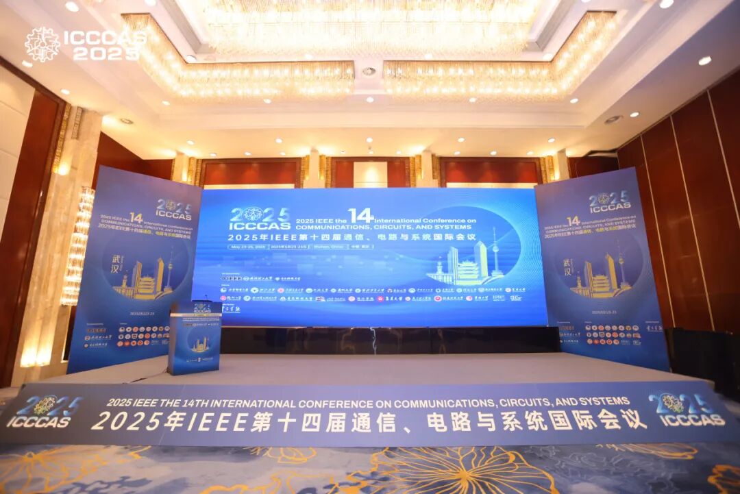
The 14th IEEE International Conference on Communications, Circuits and Systems (ICCCAS 2025) will be grandly held in Wuhan from May 23 to 25, 2025, co-hosted by IEEE, Wuhan University of Technology, and University of Electronic Science and Technology of China. A total of 170 scholars and researchers from universities and research institutions in China, Japan, Canada, South Korea, Malaysia, and other countries and regions participated in this conference.
Dr. Zhao Yi, founder of Silicon Core Technology, was invited as a keynote speaker and delivered a special report in the “3D Integrated Circuits and Advanced Packaging Technology” sub-forum, discussing the future development of high-performance integrated circuit design with many authoritative experts and representatives from well-known enterprises.
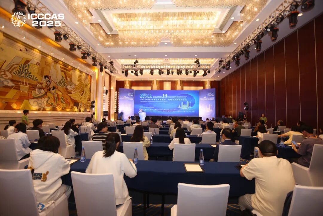
This three-day conference featured not only keynote speeches but also 12 invited reports and 11 offline sub-forums. Experts and scholars presented their latest research results and technological advancements, with several experts and professors from Peking University, Fudan University, Wuhan University, and Shanghai University of Science and Technology engaging in in-depth discussions on 3D IC and advanced packaging technology.
In his speech titled “Exploration of EDA for 2.5D/3D ICs for Advanced Packaging – A Unified Platform for Backend Physical Design Simulation and Verification,” Dr. Zhao Yi deeply analyzed the core challenges of digital backend design at advanced process nodes and shared Silicon Core Technology’s achievements in technology transformation and industrialization in the field of 2.5D/3D stacked chip design.
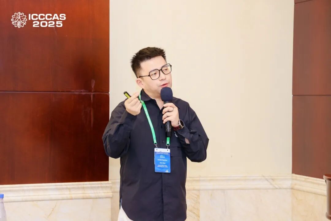
Dr. Zhao Yi, founder of Silicon Core Technology, delivers a speech
The 2.5D/3D Chiplet technology is driving the integrated circuit industry to overcome the development bottleneck beyond Moore’s Law. 2.5D packaging achieves multi-chip planar integration through silicon interposers, while 3D packaging employs TSV technology for vertical stacking of chips, both opening up new dimensions for increasing transistor density.
The 3D stacking of Chiplets represents the most advanced integration method. This “decompose-reconstruct” paradigm not only breaks through the limits of single-chip processes but also organically integrates discrete functional modules such as computing, storage, and sensing through heterogeneous integration, demonstrating significant advantages in fields like AI and HPC.
However, three-dimensional heterogeneous integration poses new challenges for EDA toolchains:
1
The traditional single-chip design process is insufficient to meet the multi-dimensional collaborative needs, lacking a comprehensive solution from architecture planning to thermal simulation.
2
System-level collaborative design requires seamless coupling simulation of multi-physical fields across chip-packaging-system, raising higher demands for cross-level electromagnetic field modeling and power analysis.
3
Stable supply chains require EDA tools to deeply embed manufacturing know-how, establishing an intelligent mapping system from process parameters to design rules.
4
The micro-bumps and hybrid bonding technologies in the packaging process pose challenges for modeling, necessitating the construction of force-magnetic-thermal multi-physical field coupling models to address failure risks caused by alignment errors and uneven thermal distribution.
The 14th IEEE International Conference on Communications, Circuits and Systems
“Three-dimensional integration is not merely a physical stacking but a system-level innovation from architecture to verification,” emphasized Dr. Zhao Yi.
As one of the few EDA companies in China capable of providing a full-process capability for 2.5D/3D stacked chip backend design, Silicon Core Technology relies on the3Sheng Integration Platform stacked chip EDA platform to build a core technological barrier. This platform, centered on the five engines of “architecture-testing design-physical design-collaborative simulation-verification,” integrates three-dimensional collaborative design architecture (chiplet-interposer-packaging) with a multi-objective collaborative optimization system (performance-cost-testability), creating a closed-loop process from architecture planning to physical realization of Chiplet design.
It is reported that the ICCCAS series of conferences was initiated in 2002 by the University of Electronic Science and Technology of China and has successfully held thirteen sessions in Singapore, Chengdu, Xiamen, Hong Kong, Japan, the United States, and other locations, becoming an internationally influential academic conference in the field of communications, circuits, and systems.
During this conference, Silicon Core Technology further demonstrated its strong capabilities in the field of advanced packaging EDA, while deepening technical exchanges with upstream and downstream industries, the company is also actively exploring new models for the integration of industry, academia, and research, looking forward to collaborating with more partners to jointly promote innovation in China’s semiconductor industry in design and manufacturing.
END
About Silicon Core Technology
Zhuhai Silicon Core Technology Co., Ltd. is mainly engaged in the research and development and industrialization of next-generation 2.5D/3D stacked chip EDA software design. The EDA for three-dimensional integrated circuits (stacked chips) design is a significant technological innovation product that achieves higher performance, higher integration, higher reliability, and lower power consumption chip systems through stacked chip design, which not only fills the gap in domestic chip EDA software but also leverages the industry trend of 2.5D/3D stacked chips to assist in upgrading the domestic chip design industry and promote the development of various chips and terminal applications in RISC-V, AI, GPU, CPU, NPU, etc.
Selected Past Issues

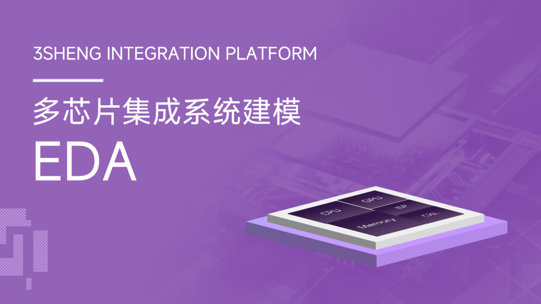
3D Stacked Chip System Modeling Tool
3Sheng Zenith
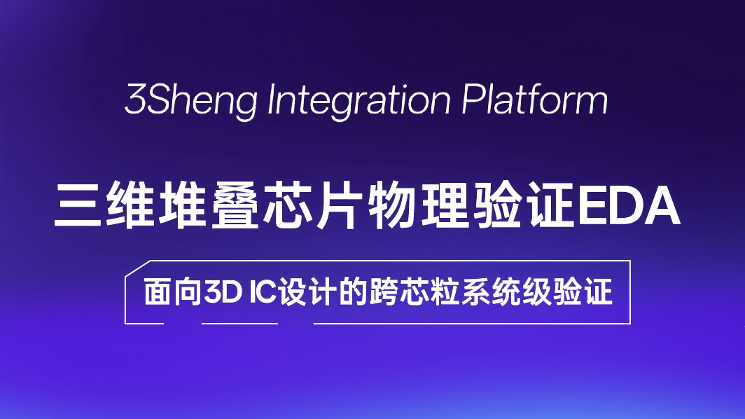
3D Stacked Chip Physical Verification Tool
3Sheng Stratify
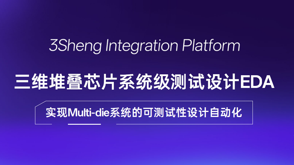
3D Stacked Chip Test Design Tool
3Sheng Ocean