Power supply design is also a very important aspect of FPGA design. The following explains the power supply design for the 7 series FPGA.
1.Introduction to FPGA Power Supply Types
The LVCMOS standards supported by the 7 series FPGA are: LVCMOS12, LVCOMS15, LVCMOS18, LVCMOS25, and LVCMOS33. Among them, LVCMOS25 and LVCMOS33 I/O standards can only be applied in HR I/O banks, while LVCMOS18, LVCMOS15, and LVCMOS12 I/O standards can be applied in both HR and HP banks.;
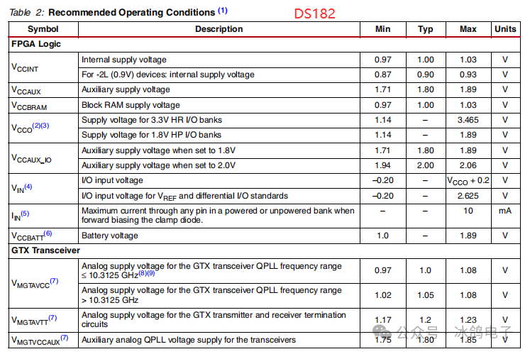
Figure 1: Common Power Supply for XC7K325T-2FFG900I and MGT Power Supply
1.Explanation of Power Supply Types for the 7 Series
The power supplies required for the normal operation of the FPGA can be divided into common power supplies and MGT power supplies.
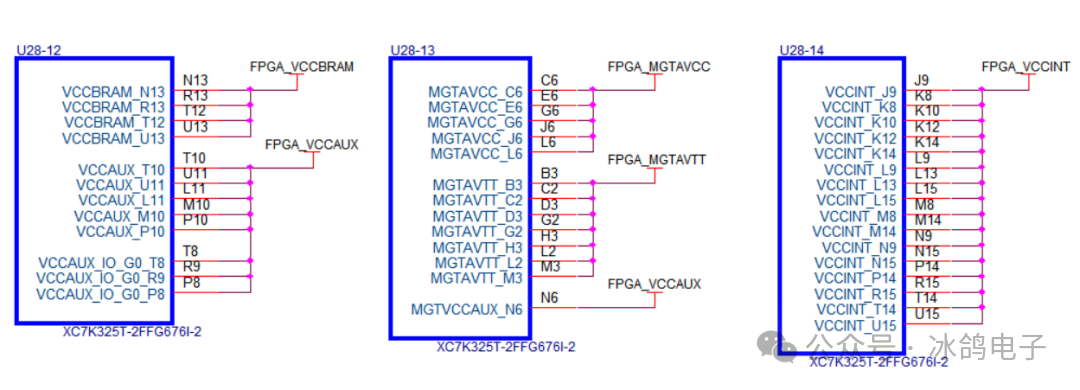
1) VCCINT
Internal core voltage of the FPGA, which powers the logic gates and flip-flops inside the FPGA, and has the highest current consumption. The range that does not damage the FPGA device is -0.5V to 1.1V.
For the Kintex-7 series -3, -2, -2LE (1.0V), -1, -1M, and -1LM, the normal operating voltage is 0.97V to 1.03V, with a recommended operating voltage of 1.00V.
For the Kintex-7 series -2LE (0.9V), the normal operating voltage is 0.87V to 0.93V, with a recommended operating voltage of 0.90V. For the Kintex-7 series -2LI (0.95V), the normal operating voltage is 0.93V to 0.97V, with a recommended operating voltage of 0.95V.
2) VCCAUX
Auxiliary power supply voltage. The range that does not damage the FPGA device is -0.5V to 2.0V. The normal operating voltage is 1.71V to 1.89V, with a recommended operating voltage of 1.80V.
3) VCCBRAM
Power supply voltage for internal Block RAM. The range that does not damage the FPGA device is -0.5V to 1.1V.
For the Kintex-7 series -3, -2, -2LE (1.0V), -1, -1M, and -1LM, the normal operating voltage is 0.97V to 1.03V, with a recommended operating voltage of 1.00V.
For the Kintex-7 series -2LE (0.9V), the normal operating voltage is 0.87V to 0.93V, with a recommended operating voltage of 0.90V. For the Kintex-7 series -2LI (0.95V), the normal operating voltage is 0.93V to 0.97V, with a recommended operating voltage of 0.95V.
4) VCCO
For the interface voltage of the HR BANK, it needs to be consistent with the signal levels of external devices. The range that does not damage the FPGA device is -0.5V to 3.6V. The normal operating voltage is 1.14V to 3.465V. The recommended operating voltage should match the external signal levels.
For the interface voltage of the HP BANK, it also needs to be consistent with the signal levels of external devices. The range that does not damage the FPGA device is -0.5V to 2.0V. The normal operating voltage is 1.14V to 1.89V. The recommended operating voltage should match the external signal levels.
5) VCCAUX_IO
IO auxiliary voltage, in Xilinx FPGA chips, serves as an independent rail to power the I/O circuits in high-performance banks, while the wide range HR bank does not have this power supply. The range that does not damage the FPGA device is -0.5V to 2.06V. The normal operating voltage is 1.14V to 1.89V/2.06V. The recommended operating voltage is 1.8V/2V.
6) VCCADC
Power supply voltage for XADC. The range that does not damage the FPGA device is -0.5V to 2.0V. The normal operating voltage is 1.71V to 1.89V. The recommended operating voltage is 1.80V.
7) MGTAVCC
Core voltage for GTX transceivers (Phase-Locked Loop power supply). The range that does not damage the FPGA device is -0.5V to 1.1V. For applications with QPLL ≤ 10.3125GHz, the normal operating voltage is 0.97V to 1.08V, with a recommended operating voltage of 1.00V. For applications with QPLL > 10.3125GHz, the normal operating voltage is 1.02V to 1.08V, with a recommended operating voltage of 1.05V.
8) MGTAVTT
Terminal matching voltage for GTX transceivers. The range that does not damage the FPGA device is -0.5V to 1.32V. The normal operating voltage is 1.17V to 1.23V. The recommended operating voltage is 1.20V.
MGTAVCC and MGTAVTT are not available in all series, for example, SPARTAN7 does not have high-speed transceivers, so these two power supplies are not present. Moreover, they have higher requirements for power supply noise, and it is recommended to use low-noise LDOs for this purpose.
9) MGTVCCAUX
Auxiliary voltage for GTX transceivers. The range that does not damage the FPGA device is -0.5V to 1.935V. The normal operating voltage is 1.75V to 1.85V. The recommended operating voltage is 1.80V.
10) MGTAVTTRCAL
Calibration voltage for GTX transceivers. The range that does not damage the FPGA device is -0.5V to 1.32V. The normal operating voltage is 1.17V to 1.23V. The recommended operating voltage is 1.20V.
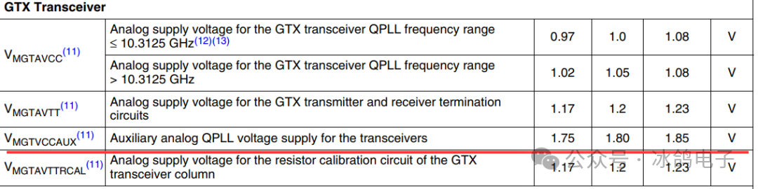
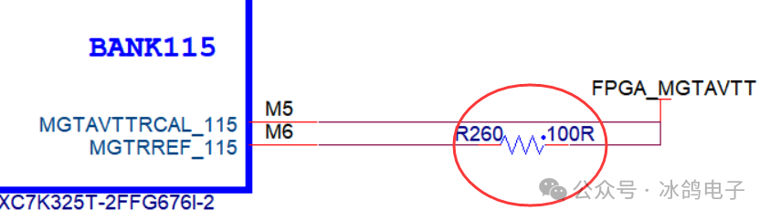
MGTAVTTRCAL pin connects to MGTAVTT power supply, and a 100Ω calibration resistor is terminated between the MGTRREF pin for calibrating the high-speed transceiver. The traces to the two pins should be of equal length, and MGTRREF does not require an additional power supply.
2.Power Supply Current Carrying Assessment
1.Current carrying capacity assessment of the FPGA
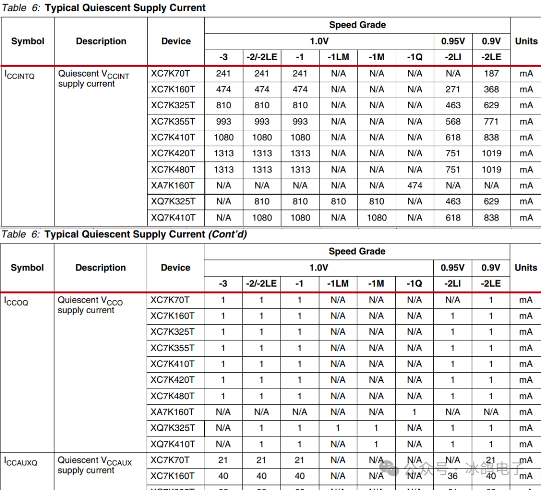
To ensure the chip powers up correctly, the minimum current needs to consider the static current plus the consumption current as shown in the table, leaving a certain margin.
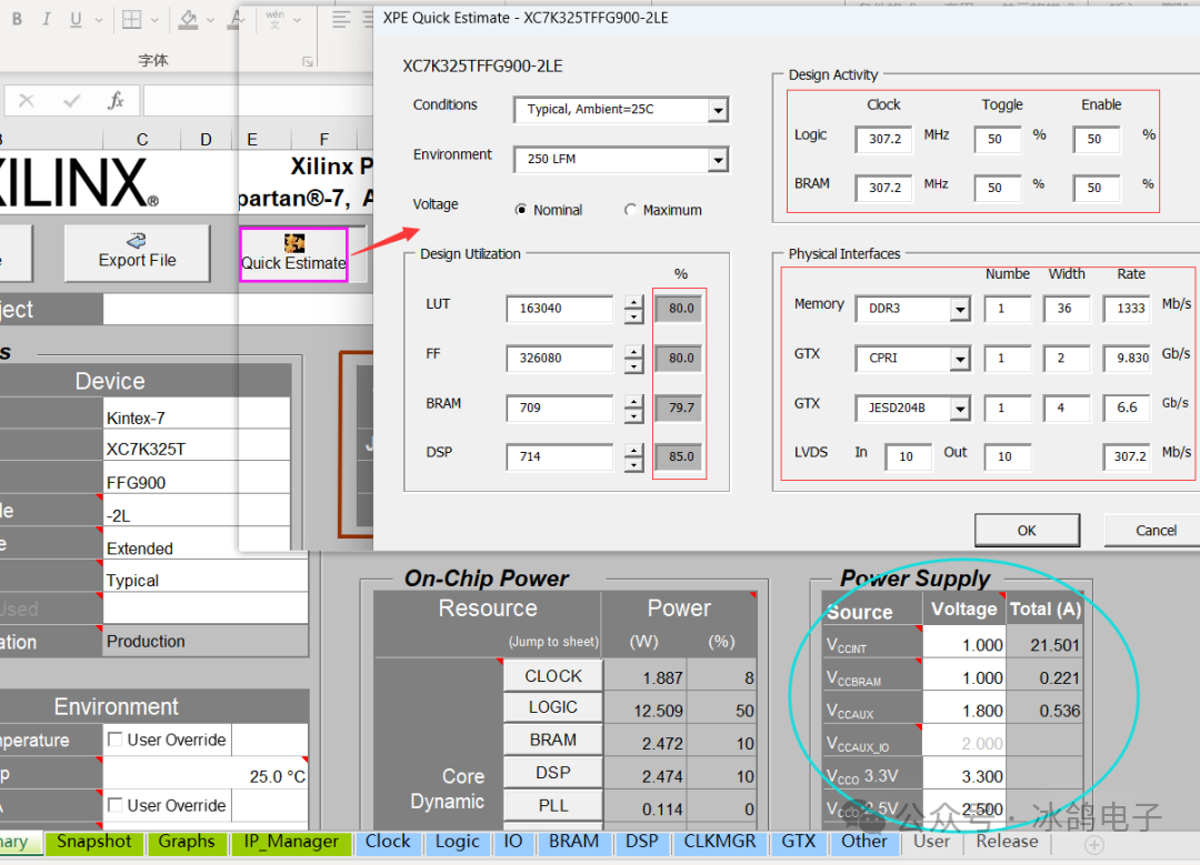
2. XPE Tool Assessment
XPE (Xilinx Power Estimator) is a power estimation tool provided by Xilinx, specifically designed to estimate the power consumption of FPGA devices before design implementation..
The XPE tool (www.xilinx.com/power) can analyze a very detailed set of parameters and conditions, including but not limited to the usage of internal logic resources, clock frequency, I/O operations, memory usage, memory interfaces, as well as voltage and temperature. Designers can predict the impact of different configurations on overall power consumption based on the various options in their actual designs using the estimates from XPE.
3.Recommended Number of Decoupling Capacitors
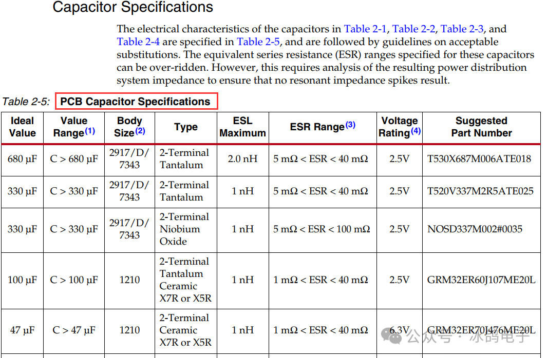
The AMD UG manual has provided the configuration for various voltage decoupling capacitors. Generally, following the configuration given in the UG manual should not pose significant issues. If space allows, it is best to have a number of decoupling capacitors greater than or equal to that specified in the manual. If conditions permit, power integrity simulation can be used, combining the models of the device and capacitors to intuitively quantify the power supply impedance situation.
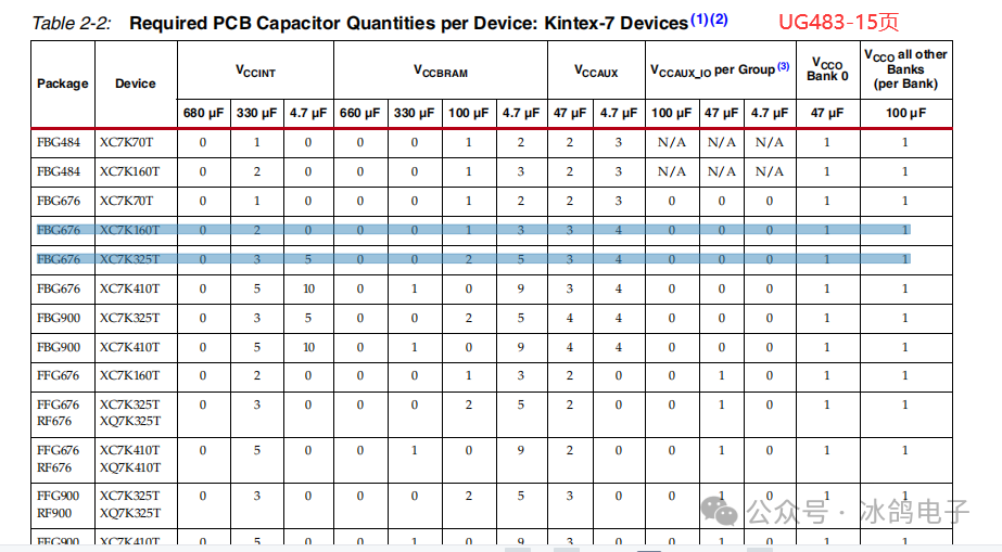
UG recommends large capacitors such as 330uF and 680uF tantalum capacitors, which can be replaced by using multiple smaller value capacitors in parallel.
4.FPGA Power-Up Timing
1.Power-Up Timing Requirements
For the Kintex-7 series FPGA, to achieve minimal power-up or power-down current consumption and ensure that the I/O remains in a tri-state during power-up, each power rail needs to have a specific power-up or power-down sequence. If the power-up is not performed according to the power supply sequence requirements of the device, it may lead to FPGA malfunction or damage.
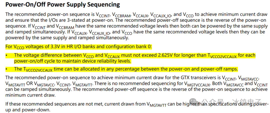
The power-up sequence is as follows:VCCINT->VCCBRAM->VCCAUX, VCCAUX_IO->VCCO, and the power-down sequence is exactly the opposite. Additionally, if the VCCINT and VCCBRAM power rails are the same, they can be powered up/down simultaneously. VCCAUX_IO and VCCAUX can also be powered up/down simultaneously with the VCCO power rail. Other power rails do not have a specific power-up sequence.
The power-up sequence for GTX transceivers is:VCCINT->MGTAVCC->MGTAVTT or MGTAVCC->VCCINT->MGTAVTT. The power-down sequence is exactly the opposite. MGTVCCAUX generally has no sequence.
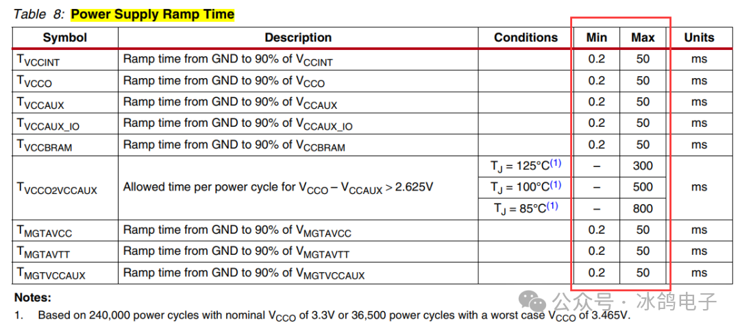
The official documentation also requires that the time for each power supply to rise to 90% is between 0.2ms and 50ms, which needs to be considered when selecting power supply chips.
The power-up timing can be referenced in the official document: “ds182_Kintex_7_Data_Sheet.pdf” – Power-On/Off Power Supply Sequencing, which provides more detailed explanations.
2.Power-Up Timing Solutions
In general, since Spartan-7 does not have MGT, its power supply structure is the simplest; Artix-7 is relatively more complex; while Kintex-7 and Virtex-7 have no significant differences in power supply structure, being the most complex.
Currently, user-designed power supply solutions for the 7 series FPGA with power-up/power-down sequences can be broadly divided into three types:
1) Using the input EN and output PGood of each power supply chip to control the sequence; — commonly used
2) Soft-start function of the power supply chip, controlling the startup time by configuring different external capacitor values;
3) Using dedicated power management chips (PMU) to control the startup/shutdown timing of each power rail of the FPGA.
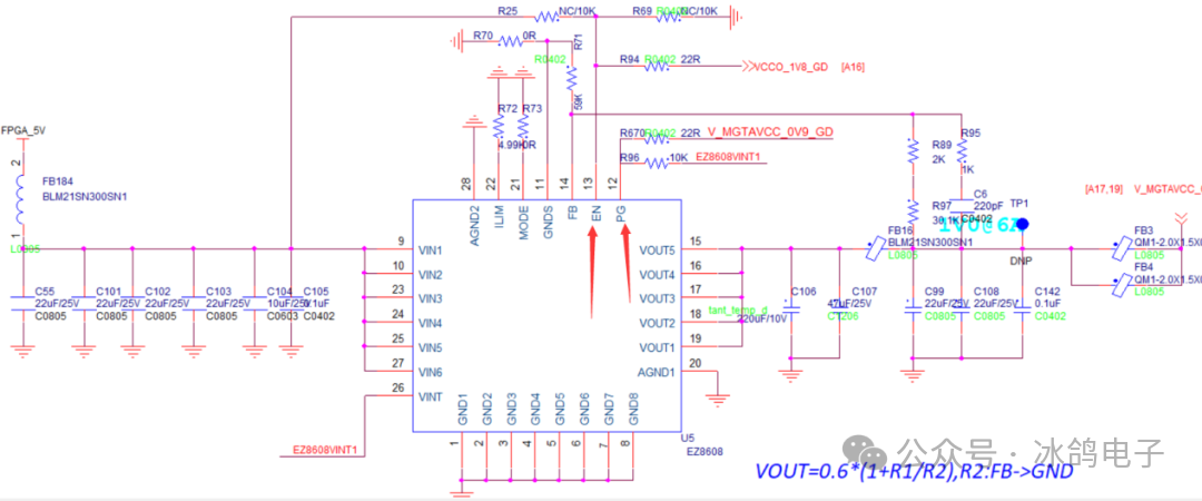
↑ In practical cases, using EN and PG to achieve power-up sequence
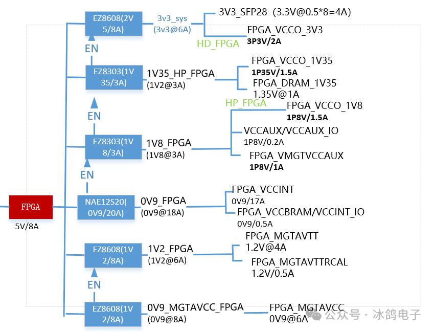
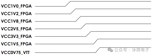
↑ Power tree for FPGA power-up timing
Reference: AMD (DS182, UG480, UG483), network information, etc.#Integrated Circuits