
PCB edge plating is a process that involves coating or plating conductive materials (usually copper) on the sides of the PCB along its height. Typically, ENIG surface treatment is used for plating at Jiepei.
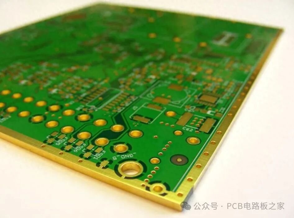
The purpose of edge plating is twofold. First, it provides reliable electrical connections. When the edge of the PCB needs to make electrical contact with another component, or when the edge serves as a connection point for external devices or connectors, the edge plating ensures consistent and reliable electrical pathways.
Secondly, edge plating enhances the rigidity and durability of the PCB. By plating the edges with conductive materials, the PCB becomes structurally more robust and less prone to failure in various aspects. It helps prevent delamination or separation of PCB layers, providing additional mechanical support and increasing the overall strength of the circuit board.
In summary, PCB edge plating involves coating or plating the sides of the PCB with conductive materials to provide reliable electrical connections and improve the structural integrity of the circuit board. This is a valuable technique for applications that require robust edge connections and enhanced durability.
1. How is the edge plating process handled?
The edge plating process requires careful handling and attention to detail to ensure successful plating and avoid potential issues. Here are some key aspects of handling the edge plating process:
Specialized equipment and skills: Proper execution of the edge plating process requires specialized equipment, such as plating tanks or machines, and skilled operators familiar with the relevant plating techniques.
Handling and preparation: Before the edges of the PCB can be plated, they need to be properly handled and prepared. This includes cleaning the edges to remove any contaminants or residues that may interfere with the plating process. The edges also need to be adequately masked or protected to ensure that plating occurs only in the intended areas.
Adhesion of the plating: The edges of the PCB need to have good adhesion with the plating material to ensure it remains securely attached throughout the lifespan of the circuit board. Adhesion-promoting techniques, such as surface roughening or applying adhesion-promoting chemicals, can be used to enhance the bond between the edges and the plating material.
Controlled soldering processes: In some cases, the edge plating process may involve soldering. It is important to carefully control the soldering process to prevent damage to the interlayer via connections. Overheating or improper soldering techniques can lead to solder wicking and potential damage to the inner layers of the PCB.
Preventing burrs: One of the main issues during the edge plating process is the formation of burrs. Burrs are undesirable metal protrusions that can occur during the plating process and may lead to short circuits or other electrical issues. Proper process control, including selecting appropriate plating parameters and using deburring techniques, is crucial for preventing burr formation and ensuring the reliability of the PCB.
By closely monitoring these considerations and taking appropriate measures, the edge plating process can be successfully executed, resulting in reliable and durable edge plating that meets PCB design requirements. Careful handling, preparation, and process control help ensure the quality and integrity of the plated edges, minimizing the risk of issues and failures.
2. Steps in the PCB Edge Plating Process
In the complex field of printed circuit board (PCB) manufacturing, the PCB edge plating process is a critical technology, especially for applications that require steadfast edge connections, unwavering conductivity, and robust protection for exposed circuit board edges. This meticulous procedure unfolds through a series of stringent steps, each playing a unique role in achieving excellent electrical connections, mechanical strength, and corrosion resistance. Let us embark on a comprehensive exploration of this process:
1. Drilling: Starting with precision, holes are carefully drilled along the edges of the PCB to accommodate the upcoming edge contacts or connectors.
2. Chemical and Electrolytic Copper Plating: The PCB begins its dual plating journey. First, a chemical copper plating bath uniformly deposits a thin layer of copper across the entire PCB, extending to the edges. This initial layer serves as a conductive foundation for subsequent electroplating work. Next, the PCB enters the electrolytic copper plating phase, where a thicker copper layer is meticulously built along the edges. This stage helps ensure conductivity and durability.
3. Etching: Following the plating process, the PCB undergoes an etching ritual aimed at removing any excess copper and outlining isolated traces. This critical step ultimately determines the precise shape and configuration of the edge contacts.
4. Surface Treatment: The edges of the PCB undergo meticulous surface treatment techniques, including micro-etching. This methodical preparation eliminates any surface oxides or contaminants, enhancing adhesion and ensuring comprehensive plating coverage.
5. Immersion Plating: The prepared edges are immersed in a plating solution, typically containing precious metals such as gold or other metals known for their excellent conductivity and corrosion resistance. The immersion plating process delicately deposits a fine layer of the selected metal onto the exposed copper surfaces, including the edges.
6. Cleaning and Drying: After plating, the PCB undergoes a rigorous cleaning procedure to eliminate any residues or contaminants. This stringent cleaning regimen ensures the integrity of the plated edges. Subsequently, the circuit board undergoes a thorough drying process, preparing it for the next stages of manufacturing.
7. Quality Inspection: The plated edge PCB then undergoes a meticulous quality inspection. This comprehensive assessment includes various critical parameters, such as plating thickness, uninterrupted continuity of edge contacts, and the identification of any anomalies or defects. This meticulous review ensures that the edge plating fully complies with specified requirements and stringent quality standards.
8. Electrical Testing (if required): Depending on the specific requirements of the PCB and the application at hand, an optional electrical testing phase may be conducted. This test aims to verify the functionality and performance of the edge contacts and the overall electrical connections, leaving no room for uncertainty.
The PCB edge plating process, while firmly rooted in traditional PCB manufacturing methods, opens a unique pathway by incorporating these specialized steps dedicated to edge plating. These meticulous measures contribute to enhancing the reliability of edge contacts, ensuring adequate plating thickness, and maintaining the overall quality of the edge plating.

Part of the eBook screenshots
【Complete Set of Hardware Learning Materials Collection】