1 What is eMMC
eMMC stands for embedded MultiMediaCard, which is a standard for flash memory cards that defines the physical architecture and access interface and protocol for storage systems based on embedded MultiMediaCard, specifically established and published by the JEDEC (Joint Electron Device Engineering Council).It is an extension of MMC with advantages such as small size, low power consumption, and large capacity, making it very suitable for use as storage media in consumer electronic devices such as smartphones, tablets, and mobile internet devices.
2 Composition of eMMC
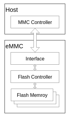
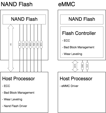
eMMC is an embedded, non-volatile storage system, primarily composed of flash memory, flash controller, and eMMC protocol interface, packaged together in a BGA format.The composition of eMMC is shown in the figure below:
Figure 1 eMMC System Structure
2.1 Flash Memory
Flash memory is a type of non-volatile memory typically used to store data, applications, and system programs.
The flash memory inside eMMC generally belongs to NAND Flash.
2.2 Flash Controller
The flash controller is mainly used to operate and manage the internal NAND Flash.
Due to the physical characteristics of NAND Flash, it requires functions such as bad block management, wear leveling, and ECC. These functions are implemented by the FTL (Flash Translation Layer).The integrated flash controller within eMMC implements functions like FTL, reducing the complexity of software development caused by the various characteristic differences of different NAND Flash models.Additionally, the flash controller provides various functions such as Cache, Memory Array, and Interleave, significantly enhancing the read and write performance of NAND Flash.
2.3 eMMC Interface
The eMMC interface mainly facilitates the connection of eMMC to the Host via the MMC bus, enabling communication with the Host and implementing the protocol logic of eMMC.
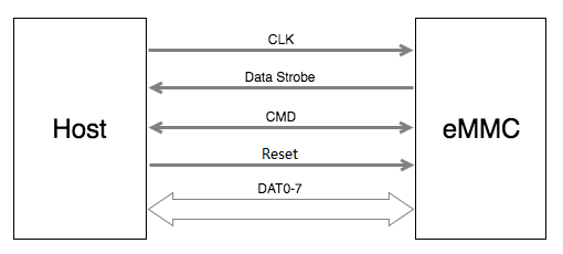
The connection between the eMMC interface and the Host is illustrated in the figure below:
Figure 2 eMMC Interface Diagram
The functions of each signal line in the interface are as follows:
CLK: Clock signal used for synchronization between Host and Device.
Data Strobe: Data latch signal, output signal from the Device, used in HS400 mode, with frequency equal to CLK, primarily for synchronizing the data output from the Device.
CMD: Used for transmitting commands from the Host and responses from the Device.
DATA0 ~ DATA7: Used for data transmission between the Host and Device.
Reset: Reset signal line, primarily used for the Host to reset the Device.
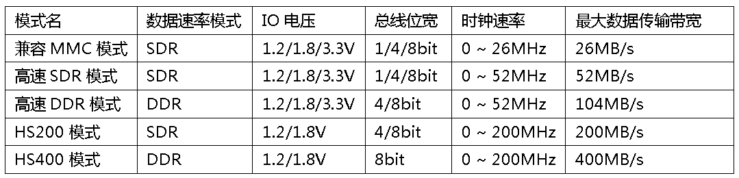
3 eMMC Working Modes
There are a total of 5 different working modes for eMMC, as detailed in the table below:
Table 1 eMMC Working Modes
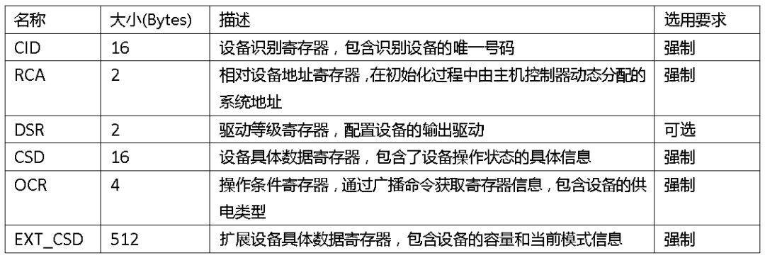
4 Internal Registers of eMMC
eMMC contains 6 different registers, mainly used to store relevant configurations and statuses of eMMC or set the configuration parameters during eMMC’s operation, facilitating the Host to query and operate eMMC.
The specific contents of the internal registers are detailed in the table below:
Table 2 eMMC Internal Registers
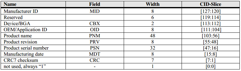
4.1 Device Identification Register
This is a 128-bit register that stores unique information about a single device, compliant with the eMMC protocol. When the device is in identification state, the information can be accessed by the Host.Specific information is shown in the table below:
Table 3 Device Identification Register
4.2 Relative Device Address Register
This is a 16-bit register; once the device is recognized, it will be assigned a relative address by the Host. When transferring data, the Host uses this information to select the device, with the default value of this register set to 0X0001.If the address changes to 0X0000, only by sending the CMD7 command can the device enter the Stand-by State to be usable.
4.3 Driver Level Register
This is a 16-bit register that specifies the device’s level, which can be set through the Host to enhance the device’s performance, such as bus length and transmission rate parameters.The specific data register for the device includes content on how this register is used. The default value for this register is 0x404.
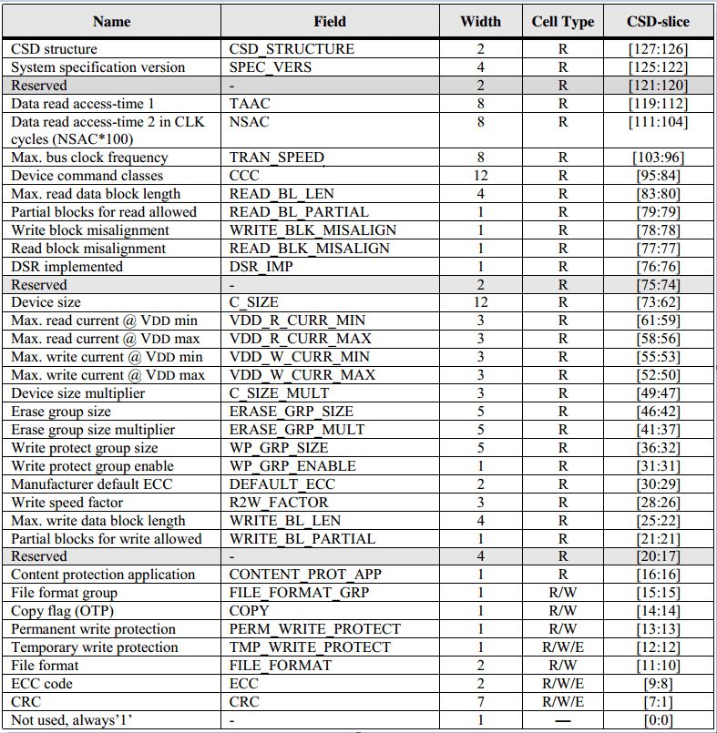
4.4 Device Specific Data Register
This is a 128-bit register that provides information on how the master controller accesses the device.It specifies the data format, error types, maximum data access time, data transfer rate, and whether the DSR register is available, among others.
The specific content is shown in the table below:
Table 4 Device Specific Data Register
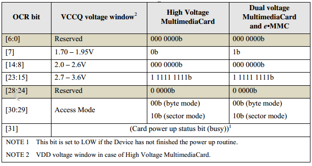
4.5 Operating Conditions Register
This is a 32-bit register that includes the voltage modes supported by the eMMC Device, data addressing modes (Byte addressing or Sector addressing), and the Busy flag.
Table 5 Operating Conditions Register
4.6 Extended Device Specific Data Register
This is a 4096-bit register that specifies the device’s attributes and selected modes.The highest 320 Bytes is the attribute block, providing capability information of the device; these attributes are read-only and cannot be rewritten.The lowest 192 Bytes is the mode block, defining the configuration information during the device’s operation. This configuration information can be rewritten through commands.
5 Comparison of eMMC with Other Memory Devices
5.1 eMMC VS NAND Flash
As previously mentioned, eMMC is a compact storage system that integrates NAND Flash, Flash Controller, and eMMC interface, providing several benefits:
1. Simplified system storage design, reducing development complexity.There are many manufacturers producing NAND Flash, including Samsung, Hynix, Micron, etc. Each manufacturer’s products have slightly different technical characteristics, requiring compatibility development, making development very complex.However, eMMC specifies a unified protocol interface, allowing us to develop based on the protocol to ensure compatibility with various manufacturers’ eMMC products, greatly simplifying the development process.
2. Fast update speed.With continuous upgrades in NAND Flash manufacturing processes, the master controller’s Flash Controller and FTL also need constant updates to support new NAND Flash.Since eMMC packages the Flash Controller and NAND Flash together, it shields differences caused by the NAND Flash manufacturing process, allowing the master controller and driver to support new technologies without extensive modifications.
3. Better read and write performance.Based on NAND Flash, eMMC incorporates technologies such as Cache and Memory Array, significantly improving read and write speeds.
Figure 3 NAND Flash VS eMMC
5.2 eMMC VS MMC
As previously mentioned, eMMC, which stands for embedded MMC, is a miniaturized version of MMC, designed for easy embedding on boards, with speed improvements from 0 ~ 52MHz to 0 ~ 200MHz.
5.3 eMMC VS UFS
Similar to eMMC, UFS is also a storage system that integrates NAND Flash, Flash Controller, and protocol interface.However, there are significant differences between the two.
1. Different protocol interfaces.eMMC uses an 8-bit parallel interface, while UFS uses a serial interface.eMMC can only perform half-duplex communication with the master controller, while UFS can achieve full-duplex communication.
2.UFS has significantly higher read and write performance than eMMC.As previously mentioned, eMMC’s use of a parallel interface limits its maximum operating frequency, currently supporting a maximum frequency of 200MHz and a maximum transmission bandwidth of 400MB/s.In contrast, UFS uses a serial interface, which can break this limit and achieve full-duplex communication, greatly enhancing read and write performance.The following is a comparison chart of the read and write performance of eMMC and UFS.
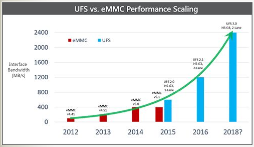 Figure 4 eMMC/UFS Performance Comparison
References
[1] eMMC Principles 2: Introduction to eMMC
http://www.wowotech.net/basic_tech/emmc_intro.html[2] eMMC Device Registers
https://linux.codingbelief.com/zh/storage/flash_memory/emmc/emmc_device_registers.html[3] MultiMediaCard
https://en.wikipedia.org/wiki/MultiMediaCard#eMMC