-
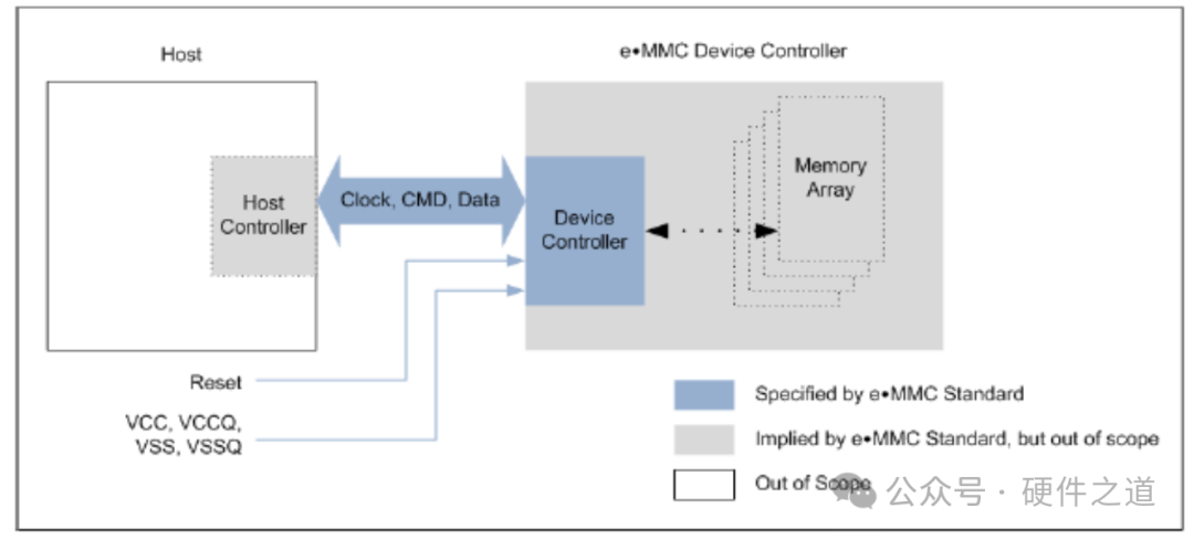
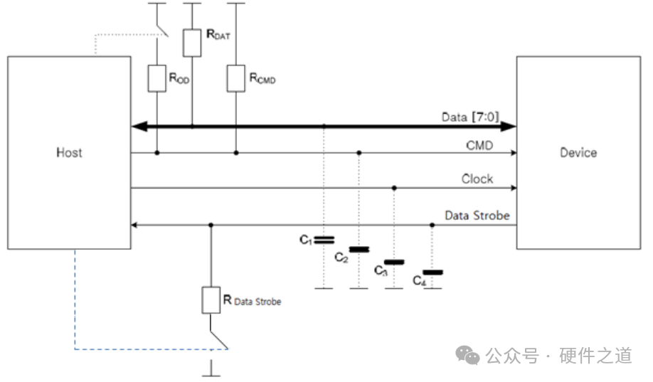
Clock: Used for synchronous clock signals.
-
Data Strobe: This signal is the clock signal output from the Device side, with the same frequency as the CLK signal, used to synchronize the data output from the Device side.
-
CMD:This signal is used to transmit the Host’s command (any operation must start with CMD, and can only be sent from host to device, and must be completed serially) and Device’s response (upon receiving the CMD sent by the host, the device will respond by sending a response through the command line, which can only be sent from device to host, and can only be transmitted serially through the command line).
-
Data[7:0]:Used for transmitting data on an 8-bit bus.
eMMC Mode
Introduction to eMMC Process
-
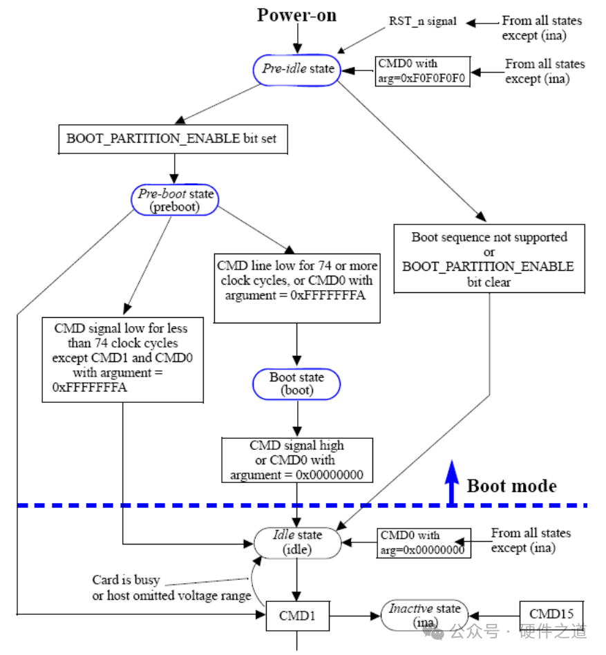
Boot Mode
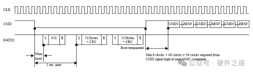
In the boot working mode, the host (usually the CPU) can keep the CMD line low or send CMD0 with the parameter 0xFFFFFFFA before sending CMD1, or under the effective condition of hardware reset, the device will enter boot mode while the host reads data from the slave (eMMC device). The data can be read from the boot area or user area, depending on the register settings. When all enabled boot data is sent to the host, the boot operation will end. After performing the boot operation, the slave will be ready for CMD1 operation. The host needs to send CMD1 to start the normal eMMC initialization routine.
-
From the protocol, it can be seen that when the host sends CMD0 to the slave or performs hardware reset on the slave, either of these conditions will cause the host to enter boot mode. After completing the boot mode, it will proceed to the next mode. -
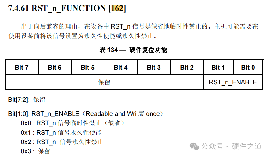
To enable hardware reset, the RST_n_ENABLE bit of the CSD register needs to be configured, and this register only needs to be configured once to take effect. -
Since most CPUs or SoCs have designated eMMC interfaces, the host usually sends CMD0 to initiate boot mode, so there is not a strong demand for starting boot mode through hardware reset, because during the internal initialization routine of the device after power-up, the device may not be able to detect the RST_n signal, as the device may not be able to complete loading the RST_n_ENABLE bit from the extended CSD register to the controller.
-
Device Identification Mode
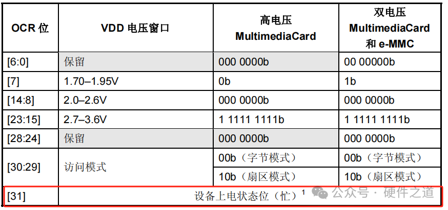
After the eMMC device completes the boot mode, it will enter the device identification mode, where the main tasks include device reset, verifying the working voltage range, and the device identification process. 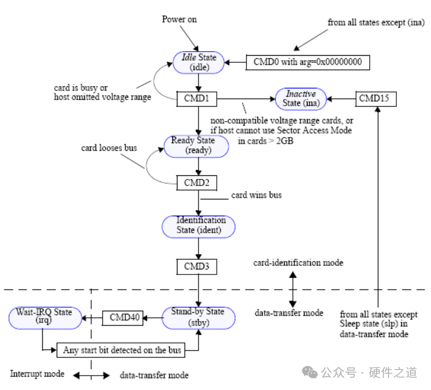
-
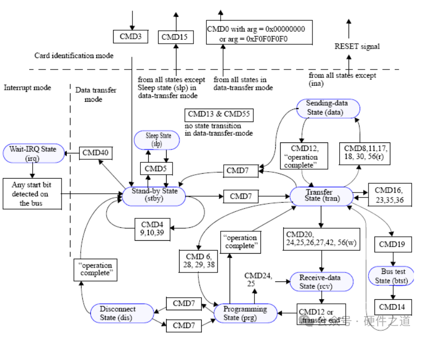
Data Transfer ModeMode
Note:
-
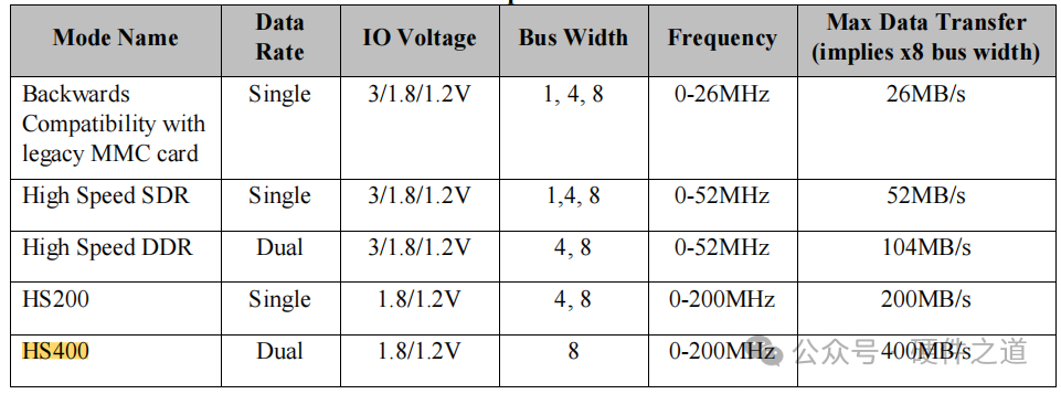
HS400 differs from HS200 mode in that HS400 uses dual-edge mode (Dual) and is only 8-bit mode.
-
It should be noted that when using HS200 or HS400 mode, the VCCQ voltage must be set to 1.8V or 1.2V to take effect.
-
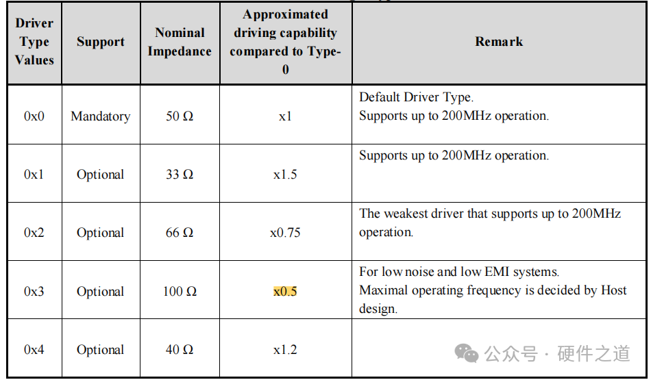
Additionally, in HS200 and HS400 modes, the I/O driving strength can be configured, with no default configuration, i.e., 0X0.
eMMC Pin Configuration
-
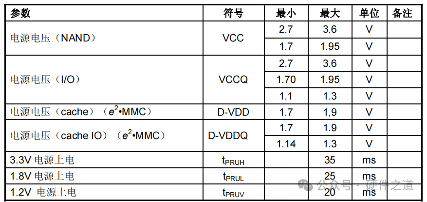
Power Voltage
-
Data and Clock Pins
Due to the open-drain output of the data, clk, cmd, and other pins of the eMMC chip during the initialization process, pull-up processing needs to be performed externally during schematic design. Additionally, since data is a bidirectional signal during high-speed transmission, monotonicity of the signal should be considered, and series resistance should be reserved at both ends of the master control and eMMC device for later debugging.
-
Wiring Requirements
-
The PCB trace impedance is controlled at 50Ω.
-
The source end should be terminated, with the termination resistor value between 22~33Ω, needing actual simulation and debugging.
-
The data trace length should not exceed 5000mil, with equal length control, especially when set to HS200 or HS400 mode.
-
Complete reference ground plane, prohibited from crossing divisions.
Typical Problem Analysis
-
File System Corruption
Regarding the usage environment of eMMC chips, they are mostly used for storing file systems or for backing up data. Therefore, designers hope for high stability of eMMC chips and that data should not be lost. How to ensure the stability of the data stored in the eMMC chip, especially when a sudden hardware power failure occurs? At this point, the eMMC chip and CPU are still performing read and write operations. If a power failure occurs, what should be done with the data during the power-off period?
The common solutions to this problem are two: the first is software configuration fsck repair, and the second is hardware configuration for reliable writing.
-
fsck (File System Check) is a tool used to check and repair file system errors, widely used in Linux and other Unix-like operating systems, to detect and repair logical and physical errors in the file system to ensure the consistency and integrity of the file system. -
fsck’s general principle: mainly checks the consistency of superblocks, inodes, and data blocks. File system writes data in sequence; if a power failure occurs in the middle, it may lead to file system inconsistency. fsck uses existing file system data to recover the parts lost during the power failure. -
Overall, the goal of fsck is to ensure the integrity and availability of the file system by detecting and repairing errors within it. It achieves repair by analyzing the structure of the file system, repairing damaged data structures, recovering lost data, and applying incomplete operations. This ensures the normal operation of the file system and provides reliable data storage and access.
-
The principle of reliable writing is that in the firmware, it guarantees that both new and old data exist simultaneously. If the write is successful, it updates to the new data; if it fails, it retains the old data.
-
Reliable writing arises from the paired page issue in NAND Flash. If a power failure occurs during the writing operation, it is very likely to corrupt previously written data.
-
The core of reliable writing is that before new data is successfully written to a certain logical address, the old data in that logical address remains unchanged. This condition provides the possibility for data recovery after a power failure.
Brief Explanation of the Paired Page Issue
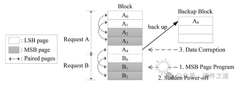
NAND flash can be divided into two types: Single-Level Cell (SLC) and Multi-Level Cell (MLC), where SLC flash can store one bit per storage cell, while MLC flash can store two or more bits. In 2-bit MLC flash, a wordline’s cell can store two paired pages and can program these two paired pages twice, referred to as the Least Significant Bit (LSB) page and the Most Significant Bit (MSB) page.
Note:
-
Due to the paired page issue in NAND Flash, a sudden power failure during write operations may corrupt previously written data. Therefore, before writing data each time, the previous data is first stored in a backup block. If the paired page issue occurs, the previous data can be restored from the backup block.
-
Because the minimum unit for read and write operations in NAND Flash is a page, the explanation above aligns with theoretical deduction. When a cell’s low page (LSB) has been programmed, if the data of the high page (MSB) is being programmed and a power failure occurs, the data successfully written in the LSB will also be corrupted.
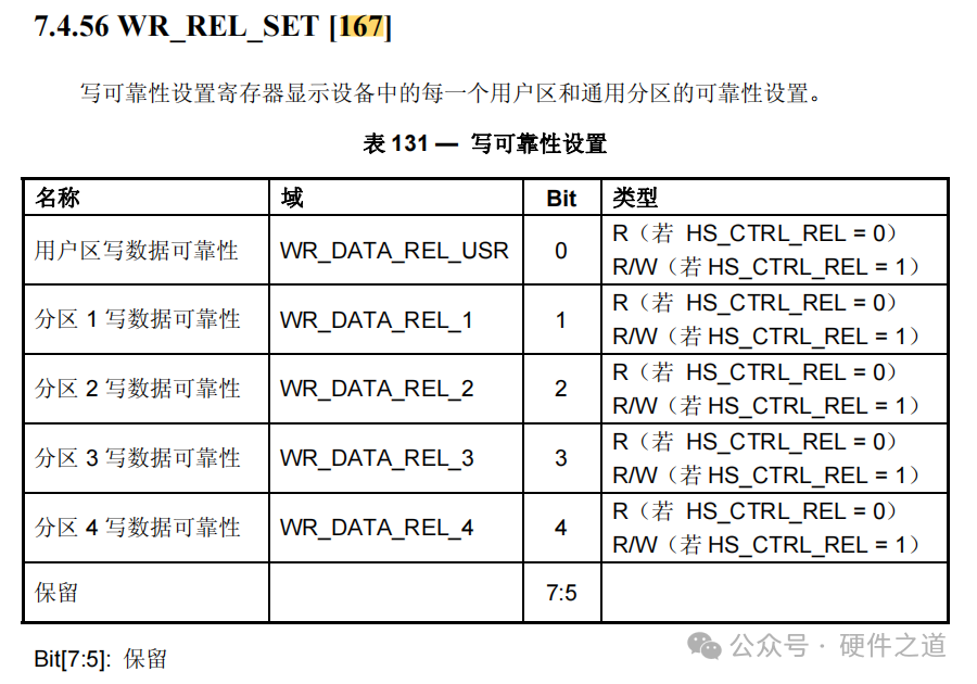
Explanation of Reliable Writing in the Protocol
-
Estimated Lifespan

Additional Explanation
-
What happens when the eMMC chip reaches the end of its lifespan?
First situation: when checking the eMMC register ecsd[268] shows that the nominal lifespan has been reached, data can still be written, but data stability will be at risk. Moreover, over time, there may occasionally be data read/write timeout issues (the eMMC protocol has read/write time requirements), and the device can still boot normally after a power cycle.
Second situation: as time goes on, there may be issues where data cannot be written, and read data cannot be corrected (similar to a large number of bit flips, causing the internal firmware algorithm of the controller to be unable to correct the data).
-
Why do some manufacturers not configure reliable writing by default?
When reliable writing is configured, it means that each time data is written, the current data will be stored in a backup block first. However, due to the poor read/write performance of some manufacturers’ backup blocks, it may affect the overall read/write speed. When reliable writing is enabled, the read/write speed may decrease by about 20% compared to when it is not enabled.