Centered around Heng Tian Yi, we can comprehensively analyze the complex and intricate process of PCB production to PCBA assembly. As a company focused on electronic manufacturing, Heng Tian Yi’s technical strength and process optimization in PCB manufacturing and SMT placement reflect the high automation, precision, and quality standards of modern electronic manufacturing.
What Are the Production Processes of PCBs
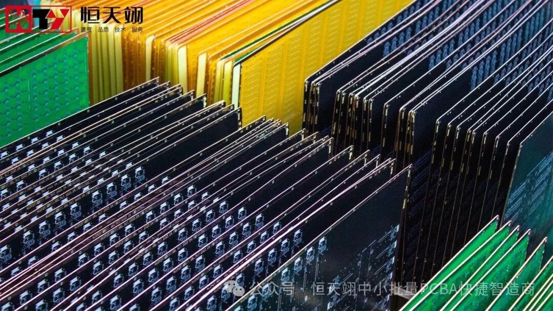
PCB Manufacturing Process
The PCB manufacturing process is a complex procedure from raw materials to finished products, involving several key steps. Taking Heng Tian Yi as an example, its PCB manufacturing process mainly includes the following stages:
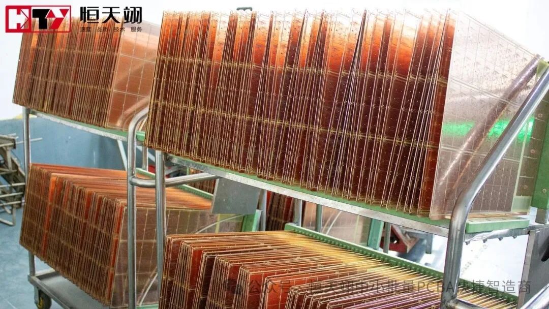
Substrate Treatment:First, the required size of PCB boards is cut from large copper-clad laminate substrates (such as FR-4 material). This process requires precise cutting equipment to ensure accuracy in size and shape.
Inner Layer Pattern Production:On the cut PCB boards, inner layer circuits are produced using photoresist and etching processes.
This process includes exposure, development, and etching to remove the unprotected copper layer, forming the desired circuit pattern.
Inner Layer AOI Inspection:After the inner layer etching is completed, automatic optical inspection (AOI) equipment is used to check the circuits, ensuring there are no short circuits, open circuits, or defects.
Lamination:For multilayer PCBs, the inner layers need to be laminated together with prepreg to form a robust stacked structure. This process requires high temperature and pressure to ensure strong interlayer bonding.
Drilling:Drilling machines are used to drill holes in the PCB for interlayer electrical connections.
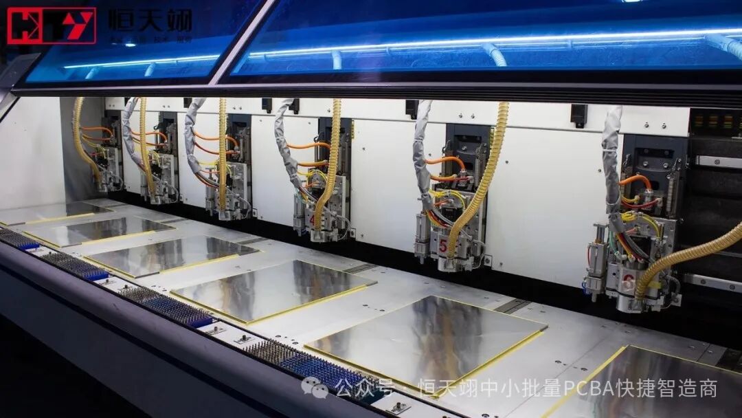
The accuracy and efficiency of drilling directly affect the performance and reliability of the PCB.
Electroplating and Panel Copper Plating:After drilling is completed, copper layers are deposited on the hole walls through electroplating to form vias. Electroplating provides a thin layer of coverage, while panel copper plating provides a thicker copper layer to enhance the reliability of the copper layer within the holes.
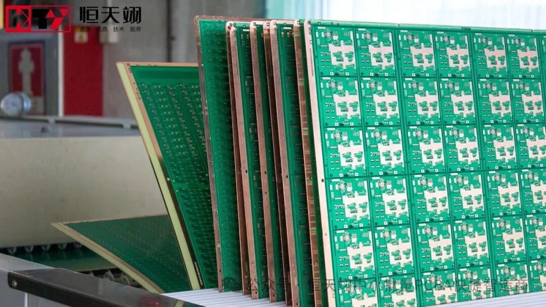
Outer Layer Pattern Production:Similar to the inner layer, the outer layer also requires the production of circuit patterns through photoresist and etching processes. This process ensures the accuracy and integrity of the outer layer circuits.
Outer Layer AOI Inspection:After completing the outer layer etching, AOI equipment is used again to check for defects in the outer layer circuits.
Solder Mask and Silkscreen:After the circuits are completed, solder mask ink is applied to protect the copper layers from oxidation and short circuits.
At the same time, reference marks or text are printed on the PCB through screen printing.
Surface Treatment:Finally, surface treatments such as tin spraying, gold plating, or OSP (Organic Surface Protection) are applied to the PCB to enhance its conductivity and corrosion resistance.
Shaping Processing:According to customer requirements, the PCB undergoes shaping processing, such as cutting and milling, to achieve specific shapes and sizes.
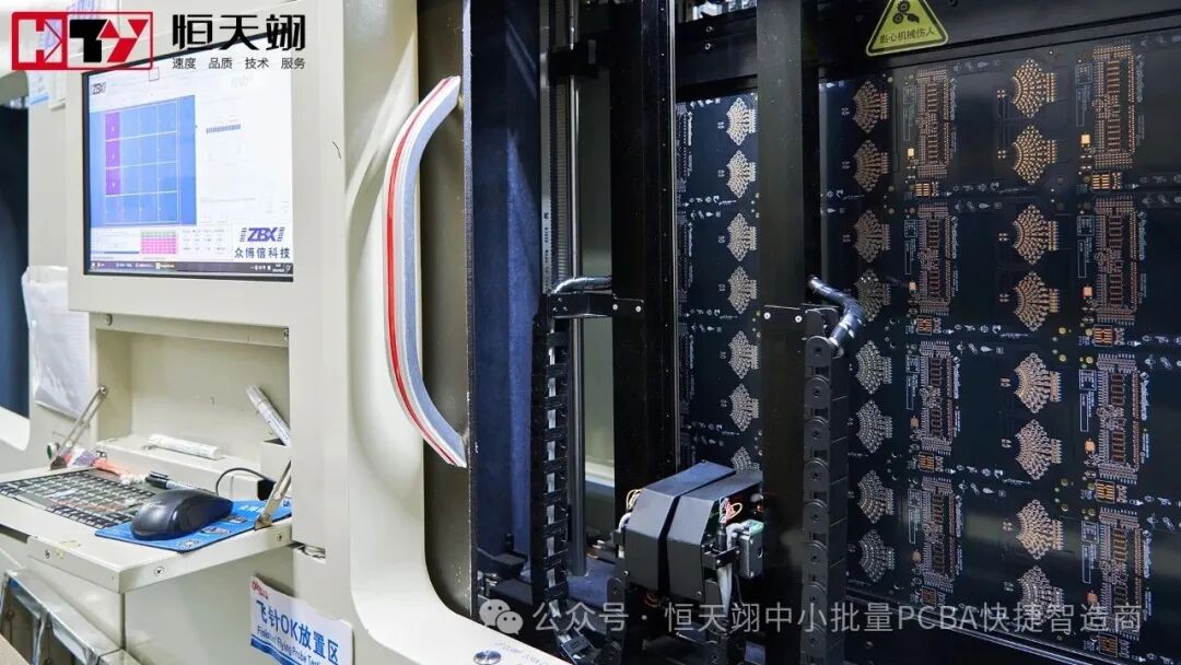
Electrical Testing:After all processing steps are completed, electrical testing is performed on the PCB to ensure its circuit connections are normal, with no short circuits or open circuits.
Final Inspection and Packaging:Finally, a final inspection is conducted to check the appearance, dimensions, and electrical performance of the PCB to ensure compliance with quality standards.
Qualified PCBs will be packaged and prepared for shipment.
Heng Tian Yi continuously optimizes its production processes in PCB manufacturing and SMT placement to improve production efficiency and product quality. For example, Heng Tian Yi has introduced a Manufacturing Execution System (MES) to track and manage the production process, enhancing production efficiency and quality control levels. Additionally, Heng Tian Yi has adopted an Automated Guided Vehicle (AGV) system for automatic material handling, reducing manual operation time and costs. Heng Tian Yi also emphasizes environmental protection and sustainable development by using low-VOC (volatile organic compounds) materials and processes to minimize environmental impact.
The processes of Heng Tian Yi in PCB manufacturing and SMT placement reflect the high automation, precision, and quality standards of modern electronic manufacturing. Through strict process control and technological innovation, Heng Tian Yi ensures the high quality and reliability of PCB and PCBA products, meeting customer needs and expectations. In the future, Heng Tian Yi will continue to explore and introduce new technologies and methods to maintain its leading position in the electronic manufacturing field.