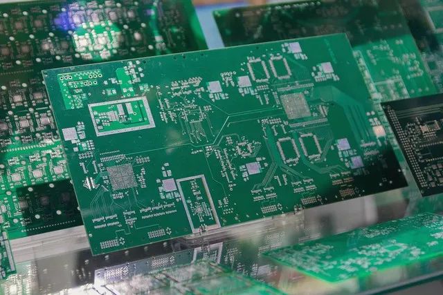
PCB manufacturing refers to the process of producing Printed Circuit Boards (PCBs). PCBs are an essential part of electronic devices, connecting various electronic components such as resistors, capacitors, and transistors through conductive patterns printed on an insulating substrate, enabling the transmission and processing of electronic signals. PCB manufacturing involves multiple steps, including design layout, substrate preparation, plating, etching, drilling, and surface treatment, ultimately forming circuit boards with specific functions, widely used in computers, communication devices, consumer electronics, medical equipment, and more. This process requires precise technology and strict quality control to ensure that the quality and performance of the circuit boards meet design requirements.
What is a PCB Manufacturing Engineer?
A PCB manufacturing engineer is a professional focused on the design, development, and manufacturing of printed circuit boards (PCBs). They are responsible for the entire process from the initial stages of circuit design to the final product production, ensuring the functionality, reliability, and production efficiency of the circuit boards. PCB manufacturing engineers play a critical role in the development and production of electronic products, and their work directly impacts the quality and market competitiveness of the products.
Main Responsibilities and Work Content of PCB Manufacturing Engineers:
1. Use Computer-Aided Design (CAD) software to create PCB layouts, determining the placement of components and routing of circuits to optimize performance and reduce costs.
2. Select appropriate substrates, copper foil, solder mask, and other materials based on the application requirements of the circuit board, ensuring stability and durability under various environmental conditions.
3. Plan the various steps of PCB manufacturing, including etching, drilling, electroplating, and silkscreen printing, ensuring each step meets quality standards and production efficiency requirements.
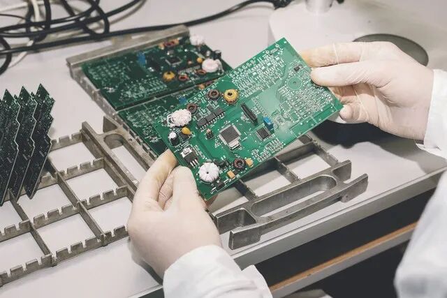
4. Create PCB prototypes and conduct functional tests to verify the correctness and performance of the design, promptly identifying and resolving potential issues.
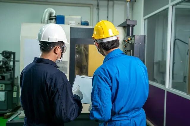
5. Supervise the mass production process, addressing technical problems that arise during production, and continuously improving production efficiency and product quality.
6. Optimize design and manufacturing processes to reduce raw material consumption and production costs while improving manufacturing efficiency and yield.
7. Write and maintain relevant technical documentation, including design specifications, process documents, and quality control standards, ensuring all operations are well-documented.
8. Collaborate closely with electronic engineers, mechanical engineers, procurement personnel, and production teams to ensure projects are completed on time and meet customer requirements.
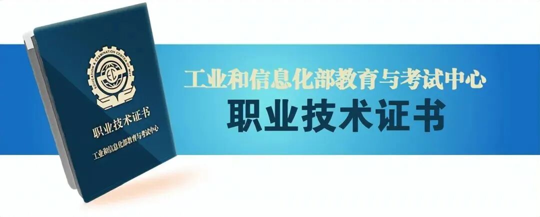
Issuing Authority for PCB Manufacturing Engineer Technical Certificate
The Education and Examination Center of the Ministry of Industry and Information Technology (MIIT) was established in 1993, formed by the merger of the original Education Center of the Ministry of Electronics, the Vocational Skills Appraisal Guidance Center of the Electronics Industry, and the Vocational Skills Appraisal Guidance Center of the former Ministry of Posts and Telecommunications. It is a public institution directly under the MIIT.
Registration Process for PCB Manufacturing Engineer Exam
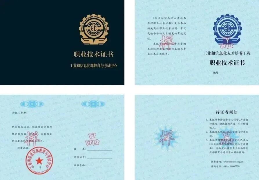
To participate in the PCB Manufacturing Engineer vocational technical certificate exam, candidates must submit relevant materials to designated units (e.g., GuoXin HongChuang Hebei Education Consulting Co., Ltd.), undergo training, and those who meet the training hours can take the PCB Manufacturing Engineer vocational technical exam. Successful candidates will receive a PCB Manufacturing Engineer vocational technical certificate issued by the Education and Examination Center of the MIIT.
Steps for registering for the PCB Manufacturing Engineer exam:
Registration Agency: Understand the registration conditions and process.
Prepare Materials: Prepare relevant materials as required by the registration agency, such as personal ID, educational certificates, etc.
Registration and Payment: Register and pay at the registration agency or designated website within the specified time.
Attend Training: Attend training courses as required by the registration agency to learn relevant knowledge and skills.
Take the Exam: After the training course, take the exam, which generally includes theoretical and practical tests.
Receive Certificate: Collect the certificate after passing the exam.
Conditions for Obtaining the Industrial Robot Application Engineer Certificate
Age Requirement: 18 years and older.
Educational Requirement: Associate degree or higher.
Professional Requirement: Graduated in network technology or computer-related majors.
Experience Requirement: At least 2 years of work experience in the industry.