4.1 What is PCB packaging, and what are its general classifications?
Answer: PCB packaging refers to the graphical representation of various parameters of actual electronic components, chips, etc. (such as component size, length and width, through-hole, surface mount, pad size, pin dimensions, pin spacing, etc.) for use in PCB design.
1. PCB packaging can be classified based on installation methods into surface mount devices, through-hole devices, mixed devices (both surface mount and through-hole), and special devices. Special devices generally refer to embedded components.
2. PCB packaging can also be classified based on function and component shape into the following categories:
SMD: Surface Mount Devices.
RA: Resistor Arrays.
MELF: Metal Electrode Face Components.
SOT: Small Outline Transistor.
SOD: Small Outline Diode.
SOIC: Small Outline Integrated Circuits.
SSOIC: Shrink Small Outline Integrated Circuits.
SOP: Small Outline Package Integrated Circuits.
SSOP: Shrink Small Outline Package Integrated Circuits.
TSOP: Thin Small Outline Package.
TSSOP: Thin Shrink Small Outline Package.
SOJ: Small Outline Integrated Circuits with J Leads.
CFP: Ceramic Flat Packs.
PQFP: Plastic Quad Flat Pack.
SQFP: Shrink Quad Flat Pack.
CQFP: Ceramic Quad Flat Pack.
PLCC: Plastic Leaded Chip Carriers.
LCC: Leadless Ceramic Chip Carriers.
QFN: Quad Flat Non-leaded Package.
DIP: Dual-In-Line Components.
PBGA: Plastic Ball Grid Array.
RF: RF Microwave Devices.
AX: Non-polarized Axial-Leaded Discretes.
CPAX: Polarized Capacitor, Axial.
CPC: Polarized Capacitor, Cylindrical.
CYL: Non-polarized Cylindrical Components.
DIODE: Diode.
LED: Light Emitting Diode.
DISC: Non-polarized Offset-leaded Discs.
RAD: Non-polarized Radial-Leaded Discretes.
TO: Transistor Outlines, JEDEC Compatible Types.
VRES: Variable Resistors.
PGA: Plastic Grid Array.
RELAY: Relay.
SIP: Single-In-Line Components.
TRAN: Transformer.
PWR: Power Module.
CO: Crystal Oscillator.
OPT: Optical Module.
SW: Switch Devices (specifically non-standard packages).
IND: Inductance (specifically non-standard packages).
4.2 What are the components of a PCB package?
Answer: Generally, a complete package is composed of many different elements, and the required components vary for different devices. The components of a package include: embedded hole size, dimension annotations, chamfer size, pads, solder mask, hole diameter, flower pads, anti-pads, pin number, pin spacing, pin pitch, silk screen lines, assembly lines, no-route areas, no-hole areas, designator characters, assembly characters, pin 1 identification, installation identification, footprint area, component height, etc. It is important to note that the following items must be included:
The components of a PCB package generally include the following elements, as shown in Figure 4-1.
(1) PCB Pads: The carrier for soldering component pins.
(2) Pin Number: The number used to match the electrical connection relationship with the component.
(3) Component Silk Screen: The identification box that describes the size of the component cavity.
(4) Solder Mask: A green oil covering that effectively protects the soldering area of the pads.
(5) Pin 1 Identification/Polarity Mark: The identifier used to locate the orientation of the component.

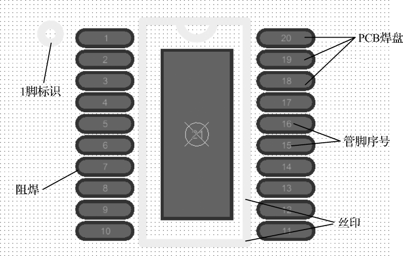
Figure 4-1 Components of PCB Packaging
4.3 What is the general process for creating a PCB package?
Answer: The steps for drawing a PCB package using Altium software are divided into two categories: surface mount type packaging and through-hole type packaging. The specific operational steps are as follows:
1. The process for creating surface mount type packaging can be summarized in the following steps:
1) Create the surface mount pad by executing the menu command “Place (P) → Pad (P)” or using the shortcut key “PP”. In placement mode, press the “TAB” key to modify the pad properties, as shown in Figure 4-2.
2) “Designator” is the pin number, and “Layer” is the pad layer property. Selecting “Top Layer” or “Bottom Layer” indicates a surface mount pad, while selecting “Multi-Layer” indicates a through-hole pad.
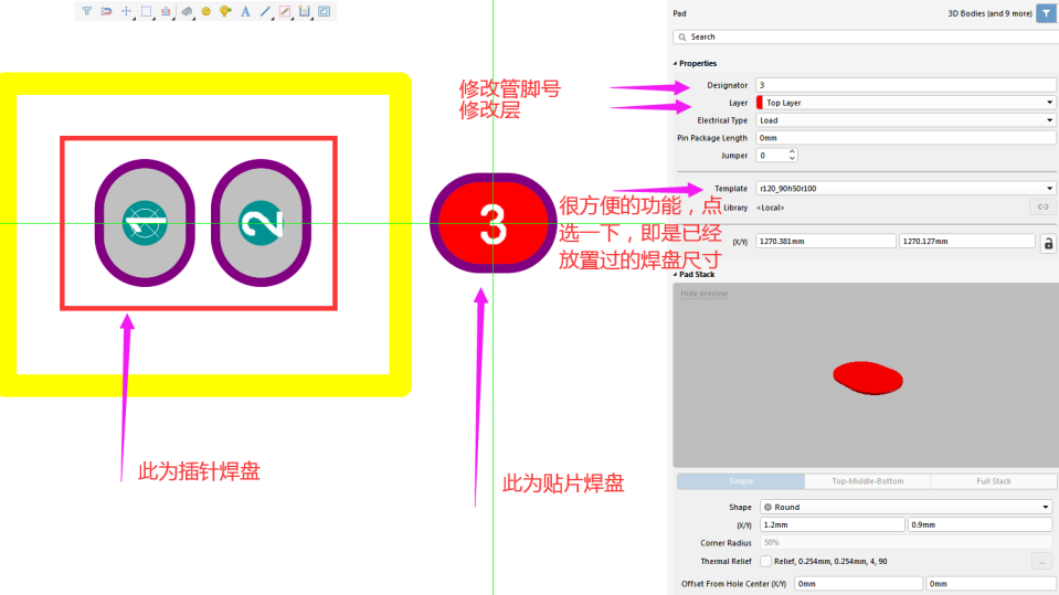
Figure 4-2 Placement of Surface Mount Pads
3) Modify the pad size by selecting the placed pad and pressing F11 to bring up the properties box. If the properties box is already present, this step can be ignored. As shown in Figure 4-3, modify the required coordinate position, rotation angle, pad type, pad size, center offset, and other defaults in the pad properties box. Modifications should only be made for special requirements. Once set, the pad is placed.
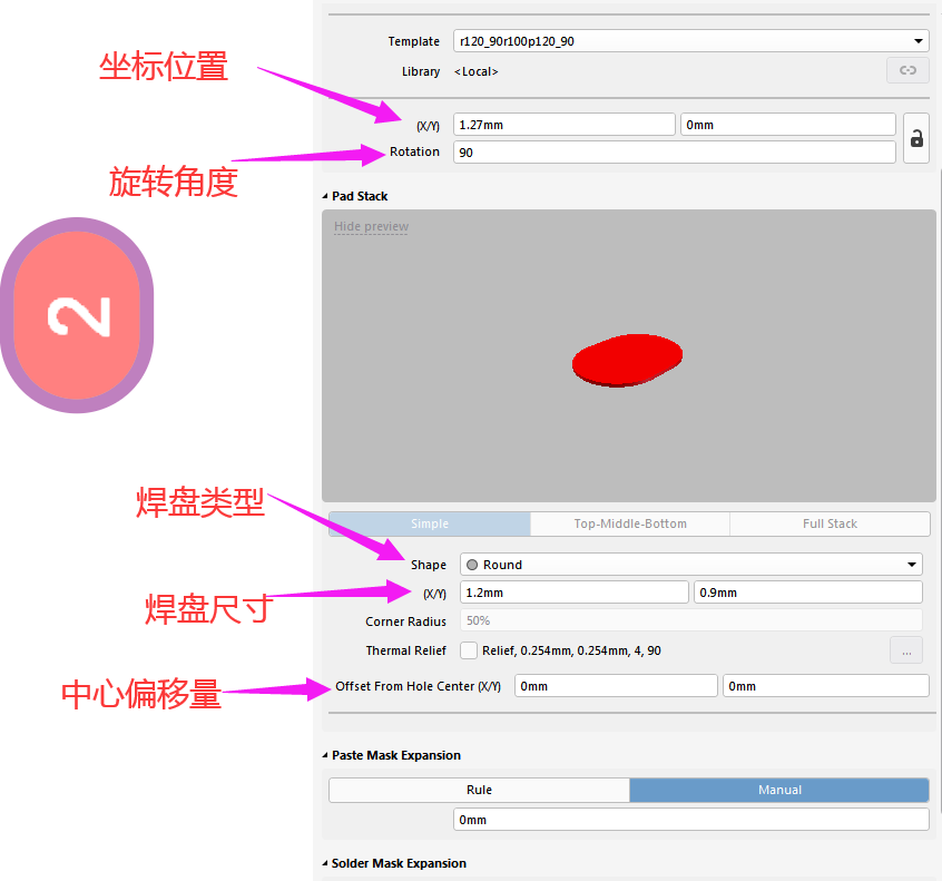
Figure 4-3 Pad Parameter Settings
4) After placing the pads in the required positions, the next step is to draw the silk screen. The chip package also needs to add the “Pin 1” label. Execute the menu command “Place → Line” to draw the approximate shape. In the Properties panel, select the drawing layer, line width, and position. The silk screen line width should be 4 mils or more (generally 0.15mm or 0.2mm), as shown in Figure 4-4.

Figure 4-4 Drawing the Silk Screen for the Package
2. The process for creating through-hole type packaging can be summarized in the following steps:
1) The process steps are the same; select “Multi-Layer” for the through-hole pad, and also set the size of the holes and pads, as shown in Figure 4-5.

Figure 4-5 Through-Hole Pad Settings
4.4 How to create a new PCB package?
Answer: Execute “File → New → Library → PCB Component Library” to create a new PCB package library.
1) Execute the menu command “File – New – Library – PCB Library” to create a new PCB library, which will generate a default file named “PcbLib1.PcbLib” and a component named “PCBCOMPONENT_1”, as shown in Figure 4-1.
2) Execute the “Save” command to rename the PCB library file to “Demo.PcbLib” for storage.
3) Double-click “PCBCOMPONENT_1” to change the name of this component; you can also right-click in the Footprints column to execute the “New Blank Footprints” command, or execute the menu command “Tools – New Blank Component” to create a new PCB package to add to the PCB package list, as shown in Figure 4-6.
Figure 4-6 Creating a New PCB Library
4.5 How to quickly switch units when creating a PCB library?
Answer: Metric is also known as the “meter system”. It is an international measurement system introduced to China after the signing of the Sino-French Commercial Treaty in 1858, originating in France. In PCB, the unit is MM (millimeters).
Imperial: A measurement system used in English-speaking countries such as the UK and the US. The main unit of length is feet, the main unit of weight is pounds, the main unit of volume is gallons, and the temperature unit is Fahrenheit. Due to various historical reasons, the imperial system is quite complex. In PCB, it is mil.
The conversion relationship between them is “1mm = 39.37mil”.
How to switch units in the PCB library? Simply execute the menu command “View → Switch Units” in the PCB package library interface, or use the shortcut key “Q” to switch units, as shown in Figure 4-7.

Figure 4-7 Creating a New PCB Library
Disclaimer:This article is an original piece by Fan Yi Education. Please indicate the source when reprinting! For submissions/recruitment/advertising/course collaboration/resource exchange, please add WeChat: 13237418207