Many embedded designs use single-board computers (SBC) and system-on-modules (SoM) based on microprocessors and microcontrollers (for example, see “Building Low-Cost Industrial Controllers with Raspberry Pi 3”). However, many more embedded applications cannot tolerate the delays caused by software-related response times.
These applications require additional performance that can only be achieved with custom hardware, and the quickest way to develop custom hardware is to use FPGAs.
This article will discuss the advantages of using SoM to develop embedded systems that require higher processing power provided by FPGAs. It will also introduce various different FPGA SoMs and discuss their use in embedded design development.
The Role of FPGA System-on-Modules
System-on-modules (SoM) can help designers develop embedded systems with custom interfaces in specific form factors without having to develop a kernel processing system from scratch. Designers can insert pre-designed and tested SoMs into pre-designed or custom carrier boards to create embedded designs that have the same functionality as completely custom designs but with much less time required for hardware development.
Using an SoM offers several advantages compared to developing hardware from scratch, including:
-
Cost savings (high non-recurring engineering costs are incurred during the development and debugging of SoC-based circuit boards)
-
Reduced design risk
-
Multiple SoC options (thanks to the pluggability of SoMs)
-
Small form factor
-
Parallel hardware and software development
The market once dominated by microprocessors and microcontrollers has now been taken over by SoMs, with through-hole and socketed components losing their dominance. Pin compatibility allows designers to choose from a range of compatible processors, picking processors with the right clock rates and appropriate on-chip memory capacities. However, as pin counts increase and surface mount packaging technologies are adopted, this design approach has become outdated, leading to the emergence of SoMs that serve the same purpose as previous pin-compatible microcontroller families.
By using an SoM as the computing platform for a project, design engineers can focus their attention and resources on developing the final application without getting lost in the myriad details of designing the computing platform. For example, at clock rates in the hundreds of megahertz (MHz), the circuit board layout for SDRAM connected to the application processor becomes increasingly difficult due to differential trace delays, noise, crosstalk, and many other challenges. However, SoM vendors have completed much of this design work before the project begins, allowing them to address these challenges and shorten time-to-market.
To choose the right SoM series for an embedded development project, various factors must be carefully analyzed, including anticipated embedded resource requirements and the need for design scalability, future adaptability, and ease of use. This helps in selecting the appropriate SoM form factor and package size, providing a rich selection of alternatives to meet known challenges and unforeseen future challenges. If the chosen SoM series includes multiple product members with compatible form factors and connector packages, it expands the design team’s options, allowing the product to better withstand the test of time.
New Types of SoM Based on Processor and FPGA SoCs
SoMs typically use SoCs with multiple application processors, but there is a new type of embedded processor SoC that integrates an FPGA, which is also suitable for SoM designs, such as the Xilinx fully programmable Zynq®-7000 SoC. The Xilinx Zynq-7000 SoC combines the software programmability of the Arm® Cortex®-A9 application processor with the hardware programmability of an FPGA. The built-in Arm microprocessor of the Zynq SoC, combined with enhanced peripherals and SDRAM memory controllers (referred to as the “processing system” or “PS” of the Zynq SoC), performs all software-based tasks typically handled by embedded microprocessors or microcontrollers, while the integrated FPGA (referred to as the “PL” or “programmable logic” of the Zynq SoC) provides hardware I/O response time and hardware acceleration for embedded tasks that require faster execution speeds.
The Xilinx Zynq SoC offers various processor configurations and speeds, and in terms of FPGA structures on the chip, even more options are available. Choosing a SoM series based on hybrid processor/FPGA SoCs (such as the Xilinx Zynq-7000 series) can expand the selection range and enhance the product’s future adaptability.
One example of such a SoM series is the TE0720 series from Trenz Electronic (Figure 1) and its corresponding SoM carrier board TE0703. All SoMs are based on a 4 x 5 cm universal form factor. The modules of the Trenz Electronic TE0720 series are based on one of the two members of the Xilinx Zynq-7000 SoC series:
-
TE0720-03-2IF based on Xilinx Zynq Z-7020 SoC
-
TE0720-03-1QF based on Xilinx Zynq Z-7020 SoC
-
TE0720-03-1CR based on Xilinx Zynq Z-7020 SoC
-
TE0720-03-1CFA based on Xilinx Zynq Z-7020 SoC
-
TE0720-03-2IFC3 based on Xilinx Zynq Z-7020 SoC
-
TE0720-03-L1IF based on Xilinx Zynq Z-7020 SoC
-
TE0720-03-14S-1C based on Xilinx Zynq Z-7014S SoC
All these SoMs have the same connector package, including three Samtec LSHM unkeyed connectors with hundreds of I/O pins, along with power and ground pins between the SoM and the carrier board.
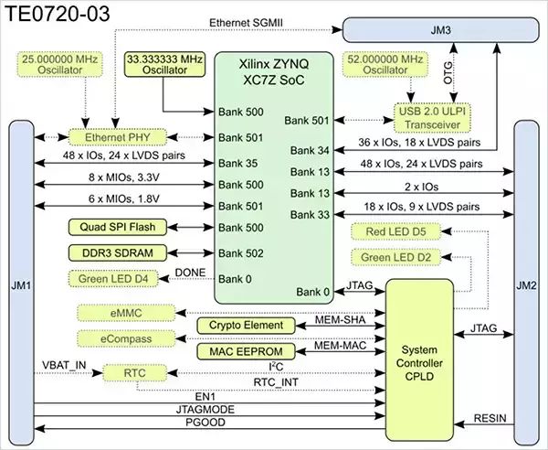
To see the flexibility of the SoM design approach, perhaps the best way is to first look at the TE0703 carrier board of the TE0720 SoM series, then trace back to the SoM through the I/O pins to see the resources of the SoM (Figure 2).

The block diagram of the TE0703 shows many important I/O functions split from the SoM board, including:
-
1 Gbit/s Ethernet
-
USB and mini USB
-
Micro SD card
-
Hundreds of I/O pins (configurable as single digital I/O pins or configured as low-voltage differential signaling pairs (LVDS))
SoMs and SBCs Each Have Their Uses
Processing speed, response time, and I/O capabilities are significant features of SoMs. However, SBCs such as the Arduino Uno and Raspberry Pi series are often integrated into embedded systems because these products also have a broad support base. Therefore, Trenz Electronic also offers corresponding versions of Arduino and Raspberry Pi development boards: TE0723-03M ArduZynq and TE0726-03M ZynqBerry based on the Xilinx Zynq-7000 SoC. These SBCs bridge the connection to many existing plug-in cards, such as Arduino shields and various Raspberry HAT and Bonnet development boards.
Compared to the FPGA capacity built into the TE0720 series Trenz Electronic SoMs (using Zynq Z-7014S and Zynq Z-7020 devices), there is a significant difference in the FPGA capacity integrated into the TE0723-03M ArduZynq and TE0726-03M ZynqBerry SBCs, which use the Zynq Z-7010 SoC. Although all Zynq-7000 SoCs use dual-core Arm Cortex-A9 processors, there are differences in the number of FPGAs on the device, as shown in Table 1:
| Xilinx Zynq SoC | Programmable Logic Units | Block RAM Capacity (Mb) | DSP Slices |
|---|---|---|---|
| Z-7010 | 28K | 2.1 | 80 |
| Z-7014S | 65K | 3.8 | 170 |
| Z-7020 | 85K | 4.9 | 220 |
Table 1: The FPGA resources provided by the Xilinx Zynq-7000 SoC (Z-7014S and Z-7020) used in Trenz Electronic’s SoMs are greater than those used in the Zynq Z-7010 in Trenz Electronic’s ArduZynq and ZynqBerry SBCs. (Data source: Digi-Key Electronics)
Additionally, the TE0723-03M ArduZynq and TE0726-03M ZynqBerry SBCs only provide 512 MB of onboard SDRAM, while the TE0720 SoM provides 1 GB.
Trenz Electronic offers various carrier boards for its SoMs, including TE0703-05, TE0706-02, TE0701-06, and TEB0745-02. These carrier boards provide many standardized I/O functions. Some carrier boards may be suitable for a specific embedded application, but the embedded system design can also be split into custom-designed carrier boards acceptable to the SoM to meet different processing needs. This flexibility highlights the advantages of using SoM series as the foundation for embedded design. The consistent standardized connector packages of SoMs allow for simple interchangeability to accommodate changes in system specifications.
Conclusion
SoMs can significantly shorten the time required for prototyping embedded systems and reduce project risks. As long as the SoM form factor and connector package are supported, SoMs with more FPGA resources can be inserted to meet growing demands. In addition, a variety of compatible SoMs based on the Xilinx Zynq-7000 SoC can combine the processing power of the dual-core Arm Cortex-A9 processor with FPGA resources, also helping to accelerate embedded design development.
This embedded design approach using SoMs not only reduces the time required for developing the hardware portion but also allows for earlier software development in the project, thereby reducing design risks. If the project scope and requirements expand, it also provides good flexibility.
About the Author
-
Ethernet Time-Sensitive Networking for Automotive ADAS Applications
-
Developer’s Festival – XDF (Xilinx Developer Forum) Beijing Registration Channel Open!
-
Understanding the Basics of Phase-Locked Loops (PLL)
-
Playing with FPGA Using Python
-
Breaking Through the Complexity of Functional Safety Design
-
Data Converter IP for Automotive ADAS SoCs
-
Extreme Intelligence Releases Industry’s Lowest Cost FPGA ADAS Solution for Near 10 Automotive Manufacturers
-
Harnessing the Power of Python: Building Interconnected Smart Products in the Simplest Way
-
[Expert Q&A] Manual Eye Scan of UltraScale+ GTH
-
2018 Xilinx National Teacher Summit Invitation
-
Xilinx Announces Acquisition of Deep Vision Technology
-
Why FPGAs Are Becoming More Important?
-
Gene Sequencing Performance Improved by 5 Times, How Did Huawei Cloud Achieve This?


