“
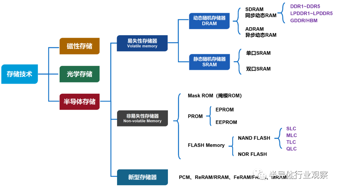
Memory is one of the important markets in semiconductors, accounting for nearly 1/3 of the semiconductor market share. Among them, in terms of sub-products of memory chips, DRAM and NAND Flash occupy over 95% of the memory chip market share, with NOR Flash accounting for 1%, and other memory chips having a smaller share.
DRAM has a fast read and write speed, but data cannot be saved after power loss, making it a mainstream solution for computer and mobile phone memory for a long time. Memory modules for computers (DDR), graphics card memory (GDDR), and mobile operating memory (LPDDR) are all types of DRAM; NAND Flash is a type of data flash memory chip that can achieve large-capacity storage, and data is not lost after power loss, but the read and write speed is slower, widely used in eMMC/EMCP, USB flash drives, SSDs, and other markets.
Looking back at the development history of memory, its technological evolution mainly depends on changes in application scenarios.
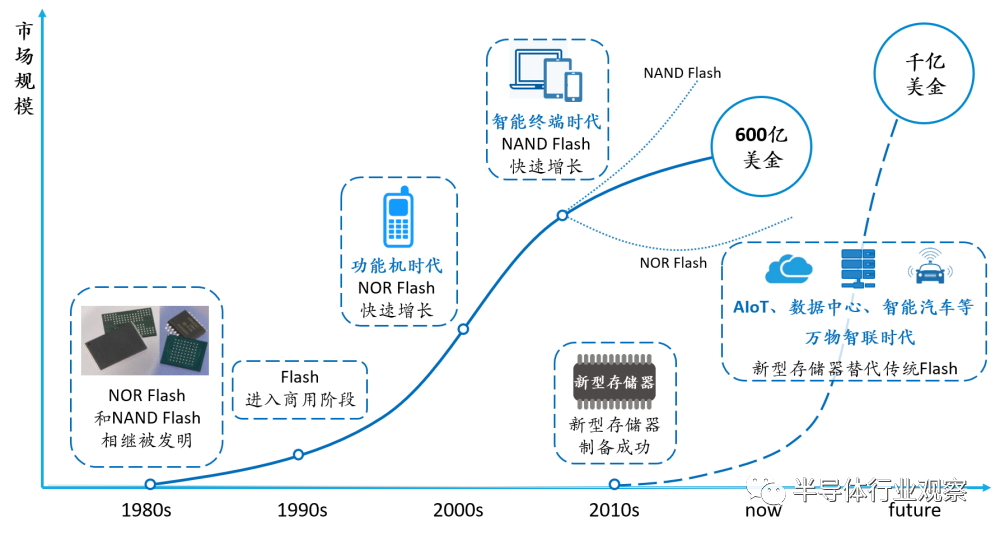
Since the 1970s, DRAM has entered the commercial market and has become the largest branch market in the storage field due to its extremely high read and write speed; the emergence of feature phones led to the explosion of the NOR Flash market; entering the PC era, people’s demand for storage capacity has grown increasingly, making low-cost, high-capacity NAND Flash the best choice.
Today, with the arrival of the era of the Internet of Everything, emerging application scenarios such as 5G, artificial intelligence, and smart cars have raised higher requirements for data storage in terms of speed, power consumption, capacity, and reliability. Although DRAM is fast, it has high power consumption, low capacity, high cost, and cannot save data after power loss, limiting its usage scenarios; NOR Flash and NAND Flash have low read and write speeds, and storage density is limited by process technology.
As the drawbacks of continuous technological innovation in traditional paths have been exposed, the market urgently needs memory products that can meet the demands of new scenarios, providing an opportunity window for new storage technologies.
At the same time, this year the storage market has gradually cooled, with prices continuously declining, and the storage industry entering a downward cycle; Intel’s closure of the Optane business has created a $2 billion high-growth market gap; the increasingly serious “memory wall” and “performance wall” issues limiting computing systems, along with the introduction of the CXL protocol, etc., have provided new storage opportunities to surpass traditional storage technology oligopolies through disruptive technological innovation paths.
According to reports published by Objective Analysis and Coughlin Associates, new storage technologies have begun to grow, and the market size is expected to reach $44 billion by 2032, ushering in a broad market space.
✦ +
+
How Much Do You Know About New Storage?
Currently, new storage technologies mainly include PCM, MRAM, FRAM, ReRAM, as well as emerging technologies such as DNA storage and Racetrack memory. At the same time, in-memory computing (computing integrated with storage) is also becoming one of the popular trends to solve current storage challenges.
Phase Change Memory PCM
Phase Change Memory, abbreviated as PCM or PCRAM.
The principle of PCM is to change the temperature to switch the phase change material between a low-resistance crystalline (conductive) state and a high-resistance amorphous (non-conductive) state.
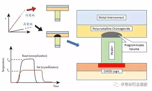
PCM Schematic Diagram (Image Source: Intel)
Characteristics of PCM Technology:
Low Latency, Balanced Read and Write Times: PCM does not require erasing previous codes or data before writing new codes, so PCM’s read and write speed is improved compared to NAND Flash, with more balanced read and write times.
Long Lifespan: PCM’s read and write process is non-destructive, so its endurance far exceeds that of flash memory, making it more reliable than traditional mechanical hard drives.
Low Power Consumption: PCM has no mechanical moving parts, and saving codes or data does not require refreshing current, so its power consumption is lower than HDD, NAND, and DRAM.
High Density: Some PCM uses amorphous transistor designs, enabling high-density storage.
Good Radiation Resistance: PCM storage technology and materials are not dependent on the charged particle state, thus having strong resistance to space radiation, meeting defense and aerospace needs.
Although PCM has many advantages, its cooling process after RESET requires high thermal conductivity, leading to higher power consumption, and since its storage principle relies on temperature to achieve resistance changes in phase change materials, it is very temperature-sensitive and cannot be used in wide temperature scenarios. Additionally, to make phase change materials compatible with CMOS processes, PCM must adopt a multi-layer structure, thus the storage density is too low to replace NAND Flash in capacity. Furthermore, cost and yield are also bottlenecks.
The well-known 3D XPoint technology, developed by Intel and Micron, is a type of PCM.
The 3D XPoint technology has achieved a revolutionary breakthrough in non-volatile memory, although its speed is slightly slower than DRAM, its capacity is higher than DRAM and is 1000 times faster than flash memory. However, its drawbacks are also evident; 3D XPoint uses a stacked structure, generally with two layers. As the number of stacked layers increases, more masks are required, and mask costs account for the largest proportion in the entire IC manufacturing industry. Therefore, from a manufacturing perspective, achieving dozens of layers of 3D stacked structures is very challenging.
With the closure of Intel’s Optane memory business, the 3D XPoint memory technology has also come to an end.
Magnetic RAM MRAM
Magnetic RAM, abbreviated as MRAM, is a technology based on the tunneling magnetoresistance effect.
The mainstream MRAM technology currently is STT MRAM, which uses the “giant magnetoresistance effect” of a tunneling layer to read bit cells. When the magnetic directions on both sides of this layer are the same, it has low resistance; when the magnetic directions are opposite, the resistance becomes very high.
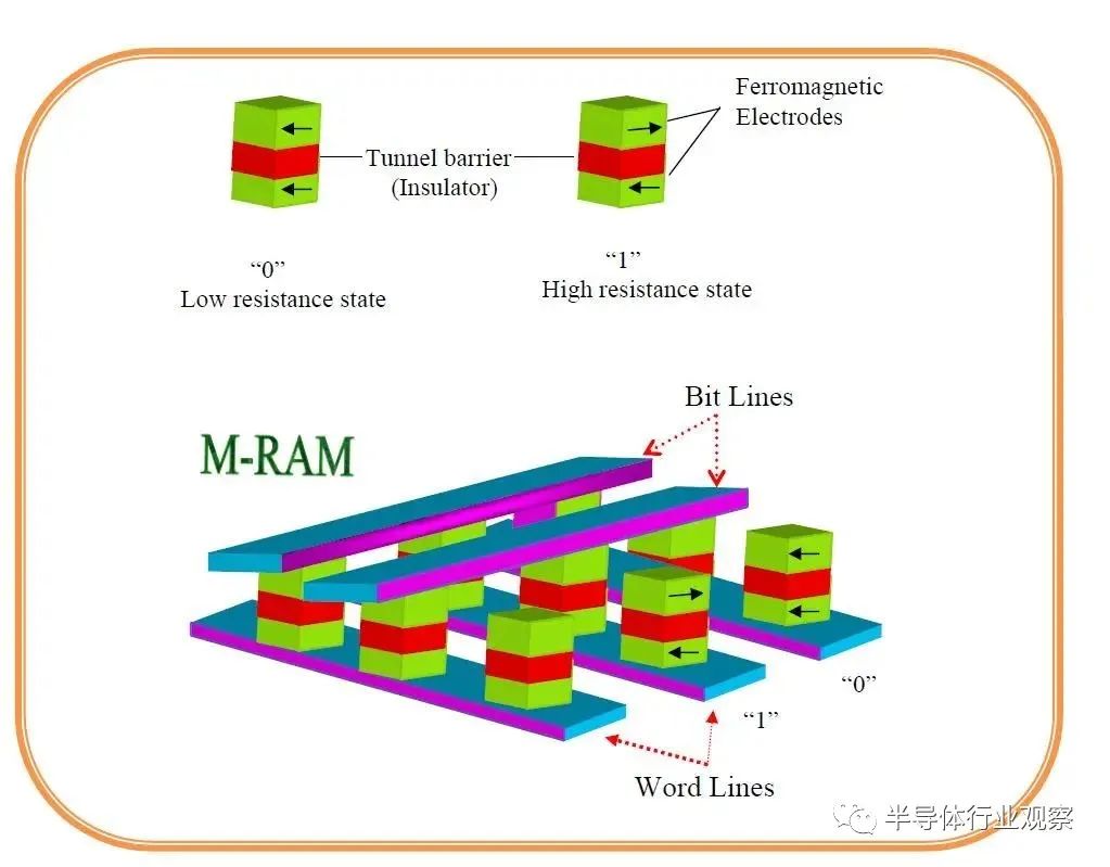
MRAM Schematic Diagram
Characteristics of MRAM Technology:
Non-volatile: The magnetism of ferromagnetic materials does not disappear due to power loss, thus MRAM has non-volatility.
Unlimited Read and Write Cycles: The magnetism of ferromagnetic materials not only does not disappear after power loss but can be considered to last indefinitely, allowing MRAM to be rewritten infinitely like DRAM.
Fast Write Speed, Low Power Consumption: The write time of MRAM can be as low as 2.3ns, and its power consumption is extremely low, enabling instant power on and off, extending battery life in portable devices.
High Integration with Logic Chips: MRAM cells can be easily embedded into logic circuit chips, requiring only one or two additional steps in the back-end metallization process that need photolithography masks. Moreover, MRAM cells can be completely fabricated in the chip’s metal layer, even allowing for 2-3 layers of cells to be stacked, thus having the potential to construct large-scale memory arrays on logic circuits.
MRAM performs well, but critical current density and power consumption still need to be further reduced. Currently, the storage cell size of MRAM is still large and does not support stacking, and the process is relatively complex, making large-scale manufacturing difficult to ensure uniformity, with storage capacity and yield climbing slowly. Before further breakthroughs in the process are achieved, MRAM products are mainly suitable for special applications with low capacity requirements and emerging IoT embedded storage fields.
Resistive RAM ReRAM
Resistive RAM, fully known as Resistive Random Access Memory, abbreviated as ReRAM or RRAM.
ReRAM is a non-volatile memory based on the reversible conversion of the resistance of non-conductive materials between high-resistance and low-resistance states under the influence of an external electric field. As the simplest storage technology in structure, ReRAM looks like a sandwich, with an insulating dielectric layer (resistive layer) sandwiched between two layers of metal, forming a metal-insulator-metal (MIM) three-layer structure.
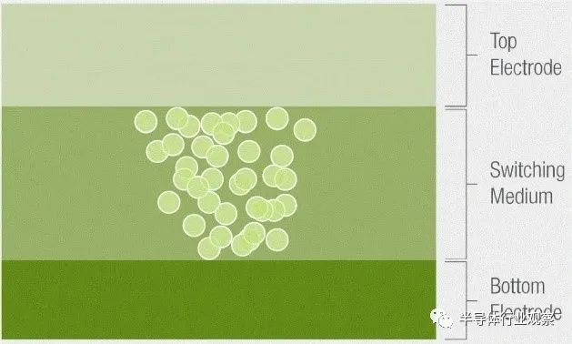
Conductive filaments can present two states in the resistive layer: a non-volatile low-resistance state or a high-resistance state, thus distinguishing and storing the “0” and “1” states.
ReRAM includes many different technology categories, with the mainstream technology routes currently being: Oxygen Vacancy Memory (OxRAM), Conductive Bridge Memory (CBRAM), Metal Ion Memory (MeRAM), and Carbon Nanotube Memory (CaRAM), usually representing 1 or 0 by moving conductive elements such as metal ions or oxygen vacancies into the bridge, or removing them from existing bridges.
Characteristics of ReRAM Technology:
High Speed: The erase/write speed of ReRAM is determined by the pulse width that triggers the resistance change, generally less than 100ns.
Durability: The read and write process of ReRAM is different from NAND, adopting a reversible non-destructive mode, greatly improving its lifespan.
Multi-bit Storage Capability: Some ReRAM materials also have multiple resistance states, making it possible for a single storage unit to store multiple bits of data, thus increasing storage density.
ReRAM can combine the read/write speed of DRAM with the non-volatility of SSD, possessing multiple advantages mentioned above, and is widely used in neuromorphic computing fields. ReRAM-based brain-like computing can also break through the bottleneck of the von Neumann computing architecture in the medium to long term, supporting various AI algorithms with high computational power and low power consumption.
Overall, ReRAM storage has significant advantages in terms of density, energy efficiency, cost, process technology, and yield among the existing new storage technologies. Additionally, ReRAM requires fewer types of materials and fewer additional masks, enabling lower production costs. The industry generally believes that ReRAM can fully meet the energy consumption, performance, and storage density requirements of applications such as neuromorphic computing and edge computing, and is expected to be widely used in AIoT, smart cars, data centers, AI computing, and other fields, being regarded as one of the best choices for achieving computing integrated with storage.
However, ReRAM devices are not yet fully mature; they still face issues such as device non-ideality, readout circuits based on high-precision analog-to-digital converters, and non-linearities in ReRAM devices that can severely reduce training accuracy after updates.
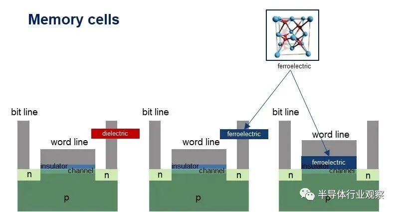
Ferroelectric RAM FRAM
Ferroelectric RAM, abbreviated as FRAM or FeRAM, uses ferroelectric crystal materials as storage media, utilizing the characteristic hysteresis loop of the voltage and current relationship of ferroelectric crystal materials to achieve information storage.
FRAM Structure Diagram
Characteristics of FRAM Technology:
Non-volatile: Data is not lost after power loss, making it a non-volatile memory;
Fast Read and Write Speed: Data can be written without delay and can be overwritten;
Long Lifespan: Repeated read and write cycles can reach trillions, providing strong durability and long lifespan;
Low Power Consumption: Low standby current, no need for backup batteries, no need for charging pump circuits;
High Reliability: Compatible with CMOS processes, wide operating temperature range, and high reliability.
FRAM products combine the non-volatile data storage characteristics of ROM with the unlimited read/write, high-speed reading, and low power consumption advantages of RAM. FRAM products include various interfaces and densities, such as industrial standard serial and parallel interfaces, industrial standard packaging types, and densities of 4Kbit, 16Kbit, 64Kbit, 256Kbit, and 1Mbit.
With its numerous characteristics, FRAM is becoming one of the future directions for memory development. According to the report “2022-2027 China FRAM (Ferroelectric RAM) Industry Market Depth Research and Development Prospects Forecast Report” released by New Thinking Industry Research Center, FRAM has low storage density and limited capacity, making it unable to completely replace DRAM and NAND Flash, but it has development potential in scenarios with low capacity requirements, high read/write speed requirements, high read/write frequency, and long lifespan requirements. FRAM can be applied in consumer electronics, such as smartwatches, smart cards, and IoT device manufacturing; in the automotive field, such as advanced driver assistance systems (ADAS) manufacturing; and in industrial robotics, such as control system manufacturing.
The mainstream ferroelectric materials currently are lead zirconate titanate (PZT) and bismuth strontium titanate (SBT), but they have fatigue degradation issues and cause environmental pollution. Recently, hafnium oxide (HfO2) has been found to have ferroelectric phases, and the ferroelectric phase can be stabilized by doping silicon (Si) into HfO2, without polluting the wafer factory. Although HfO2 is not yet used in FRAM production, it has broad prospects, and the industry is researching this technology route.
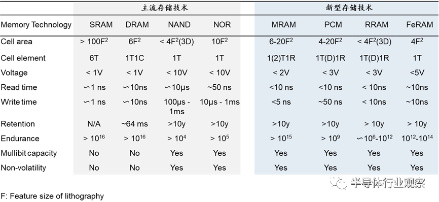
Comparison of Mainstream Storage Technologies and New Storage Technologies
New memory technologies have been emerging for decades, and now they have reached a critical period of more important performance in more applications. Through the comparison of various storage technologies above, it can be seen that new storage technologies have significant advantages, possessing super performance, latency comparable to memory, as well as ultra-long lifespan and reliability, and high-temperature resistance.
As future process miniaturization and economies of scale will promote price reductions, emerging memory is expected to be used as independent chips and embedded in ASICs, microcontrollers (MCUs), and even processing units, making it more competitive than existing memory technologies.
At the same time, the development of new storage technologies also promotes innovation and iteration in computing integrated with storage technologies.
Breakthrough in Computing Integrated with Storage?
Under the von Neumann architecture, storage units and computing units are separated, and the process of moving data consumes a large amount of time and energy. Due to the different process routes of processors and memories, the data access speed of memory cannot keep up with the data processing speed of CPUs, and performance has lagged far behind processors. Therefore, the von Neumann architecture has inherent limitations in data processing speed and energy efficiency, which is known as the “memory wall”.
The computing integrated with storage architecture eliminates the delays and power consumption caused by data access by integrating storage and computing units, making it one of the best solutions to solve the memory wall problem, achieving higher computing power and higher energy efficiency.
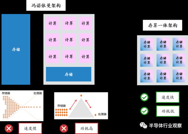
Computing Integrated with Storage Breaks Through the Memory Wall
(Image Source: Yunxiu Capital)
In the current computing integrated with storage technology paths, there are both solutions using traditional memories such as DRAM, SRAM, NAND, and solutions using new memories such as ReRAM, PCM, and MRAM.
The former, due to the different manufacturing processes of memory and logic computing units, cannot achieve good integration, currently can only achieve near-storage computing, still facing the memory wall problem, and may even lead to performance loss due to interconnection issues. Moreover, since SRAM and DRAM are volatile memories that require continuous power supply to retain data, they still have power consumption and reliability issues.
The latter combines non-volatile new storage, which can complete matrix multiplication operations within the array using Ohm’s Law and Kirchhoff’s Law without moving weights in and out of the chip. New storage is used to store data through resistance changes, and the voltage loaded on the memory equals the product of resistance and current, meaning each unit can achieve a multiplication operation, and summing them up can achieve matrix multiplication, so new storage inherently possesses the properties of both storage and computation.
In this case, the same unit can complete both data storage and computation, eliminating the delays and power consumption caused by data access, representing a true sense of computing integrated with storage.
In addition to the four major new storage technologies mentioned above, new emerging technologies such as Racetrack memory and DNA storage are also continuously emerging.
Racetrack Memory
Racetrack memory, also known as domain-wall memory (DWM), is a new memory technology that uses atoms in magnetic nanotubes to store information, reading 16 bits of data through a single transistor, thus its read and write speed is 100,000 times faster than flash memory.
At the same time, Racetrack memory can store a large amount of data that can be accessed very quickly, and its storage density is higher than existing flash memory, close to current hard disk technology, and can be used as universal memory.
Compared to other memory technologies, Racetrack memory may have unparalleled density, being solid-state like flash memory, with no heavy moving parts, and is non-volatile, meaning it can retain data even after power loss.
These devices can store more information in the same space, requiring much less power and generating much less heat, and almost do not wear out. As a result, massive personal storage contents can run for weeks on a single battery, and these contents can last for decades without worrying about damage.
Racetrack memory is still in the early stages of research, and so far, most studies on Racetrack storage have focused on 2D devices. Scientists are exploring many different methods to establish 3D Racetrack storage. Achieving three-dimensional structured Racetrack memory will not adhere to Moore’s Law, providing new possibilities for developing lower-cost, faster devices.
DNA Storage
In search of a more efficient storage medium, researchers have turned their attention to DNA, the carrier of genetic information in nature.
DNA storage is a storage technology that uses the biological macromolecule DNA as a carrier of information, with advantages of high capacity, high density, low energy consumption, and long storage time.
From a technical perspective, DNA storage has been proven to be feasible.
Recently, a synthetic biology team from Tianjin University innovated a DNA storage algorithm, storing ten selected Dunhuang murals in DNA, and verified through accelerated aging experiments that the mural information can be preserved for a thousand years at room temperature in the lab and for twenty thousand years at 9.4°C.
This technology not only confirms that DNA is a reliable storage medium but also ushers information storage technology into a new era. DNA storage technology is more suitable for storing important but infrequently accessed and retrieved “cold data.” Theoretically, “cold data” can be preserved for over a thousand years with nearly zero energy consumption. In the future, DNA storage is likely to become the primary storage medium for massive cold data storage.
DNA storage is an emerging technology that deeply integrates multiple disciplines, and significant breakthroughs have been made in DNA storage research in recent years. Researchers have been using DNA to manage data in various ways, striving to understand massive data. However, the practical application of DNA storage technology still faces some technical challenges, and turning laboratory samples into market products requires collaboration among research institutions, universities, and enterprises.
✦ +
+
Final Thoughts
As the market and technology continue to evolve, AI, 5G, IoT, and Industry 4.0 are driving explosive growth in data volume, with new computational demands pushing storage towards higher capacity, higher read/write cycles, faster read/write speeds, and lower power consumption.
As mentioned above, when the drawbacks of continuous technological innovation in traditional paths have been exposed, the market urgently needs memory products that can meet the demands of new scenarios, providing an opportunity window for new storage technologies.
However, even though current mainstream storage technologies have many limitations and challenges, and numerous new storage technologies are emerging, it is still too early to say who will prevail. Although the future prospects of new memory technologies are bright, they still find it challenging to penetrate some entrenched technical markets. Even if economic benefits improve, new memory technologies will find it difficult to quickly overturn the dominance of existing markets; rather, under the current market status and circumstances, new storage technologies, through disruptive technological innovation paths, have found an opportunity to catch up with traditional storage technology oligopolies.
The reproduced content only represents the author’s views
It does not represent the position of the Institute of Semiconductors, Chinese Academy of Sciences
Editor: Qian Niao