Programmable Logic Devices (PLDs) originated in the 1970s and are a new type of logic device developed based on Application-Specific Integrated Circuits (ASICs). They are the main hardware platform for digital system design today, characterized by being fully configurable and programmable by users through software to perform specific functions, and can be repeatedly erased and rewritten. When modifying and upgrading PLDs, there is no need to change the PCB circuit board; instead, modifications and updates are made on the computer, transforming hardware design work into software development, shortening the system design cycle, enhancing implementation flexibility, and reducing costs. This has made PLDs popular among hardware engineers, leading to a significant PLD industry scale.
Currently, common PLD products include: Programmable Read-Only Memory (PROM), Field Programmable Logic Array (FPLA), Programmable Array Logic (PAL), Generic Array Logic (GAL), Erasable Programmable Logic Array (EPLA), Complex Programmable Logic Device (CPLD), and Field Programmable Gate Array (FPGA). PLD devices can be further categorized by scale into Simple PLD (SPLD), Complex PLD (CPLD), and FPGA. Their internal structural implementation methods vary. Programmable Logic Devices can be classified into three categories based on the granularity of the basic unit:
① Small granularity (e.g., “sea of gates” architecture),
② Medium granularity (e.g., FPGA),
③ Large granularity (e.g., CPLD).
Based on programming technology, they can be divided into four categories:
① Fuse and antifuse programming devices,
② Erasable Programmable Read-Only Memory (UEPROM) programming devices,
③ Electrically Erasable Programmable Read-Only Memory (EEPROM) programming devices (e.g., CPLD),
④ SRAM programming devices (e.g., FPGA).
In the technology classification, the first three categories are non-volatile devices, meaning that after programming, the configuration data is retained on the device; the fourth category is volatile, meaning that configuration data is lost after power-off, requiring reconfiguration each time power is restored.
History of the Development of Programmable Logic Devices
The development of programmable logic devices can be divided into four stages: the first stage from the early 1970s to the mid-1970s, the second stage from the mid-1970s to the mid-1980s, the third stage from the 1980s to the end of the 1990s, and the fourth stage from the end of the 1990s to the present. In the first stage, programmable devices included only simple PROM, ultraviolet erasable PROM (EPROM), and electrically erasable PROM (EEPROM). Due to structural limitations, they could only perform simple digital logic functions. The second stage saw the emergence of slightly more complex devices such as Programmable Array Logic (PAL) and Generic Array Logic (GAL), officially referred to as PLDs, capable of performing various logic operations. A typical PLD consists of “AND” and “NOT” arrays, using “AND-OR” expressions to implement arbitrary combinational logic, allowing PLDs to perform a large number of logic combinations in product-sum form. In the third stage, Xilinx and Altera introduced FPGA and extensible CPLD, respectively, which are similar to standard gate arrays, improving the speed of logic operations and featuring flexible architecture, high integration, and wide applicability, combining the advantages of PLDs and general gate arrays, capable of implementing ultra-large-scale circuits. The programming method is also very flexible, making them the preferred choice for product prototype design and small to medium-scale (generally less than 10,000) product production. During this stage, CPLD and FPGA devices made significant advancements in manufacturing processes and product performance, reaching 0.18 processes and millions of gates. The fourth stage saw the emergence of SOPC and SOC technologies, resulting from the integration of PLD and ASIC technologies, encompassing real-time digital signal processing technology, high-speed data transceivers, complex computations, and embedded system design technologies. Xilinx and Altera also launched corresponding SOCFPGA products, with manufacturing processes reaching 65, and system gate counts exceeding one million. Moreover, the logic devices of this stage embedded high-speed multipliers, Gbits differential serial interfaces, PowerPC microprocessors with clock frequencies up to 500MHz, soft cores like MicroBlaze, Picoblaze, Nios, and NiosII, achieving a perfect combination of software requirements and hardware design, as well as high speed and flexibility, surpassing the performance and scale of ASIC devices and the traditional concept of FPGA, expanding the application range of PLDs from chip-level to system-level. Currently, the concept of on-chip programmable based on PLD is still evolving.
Development Tools
The development of high-complexity PLD devices largely relies on Electronic Design Automation (EDA). PLD EDA tools are primarily software-based, encapsulating typical unit circuits into fixed modules and forming standard hardware description languages (such as HDL) for designers to use. Designers consider how to assemble software libraries and packages to build functional modules or even complete systems that meet requirements. PLD development software needs to automatically complete tasks such as logic compilation, simplification, partitioning, synthesis and optimization, layout and routing, simulation, and adaptation compilation and programming download for specific target chips. Typical EDA tools must include two special software packages: synthesizers and adapters. The synthesizer’s function is to compile, optimize, convert, and synthesize the HDL, schematics, or state diagrams completed by the designer on the EDA platform for a specific system project, targeting given hardware system components. As the scale of development increases exponentially, it is necessary to shorten the compilation time of PLD development software, improve its compilation performance, and provide rich intellectual property (IP) core resources for designers to utilize. Additionally, the user-friendliness of the PLD development interface and the complexity of operations are also important factors in evaluating its performance. Currently, in the PLD industry, the development tools provided by various chip vendors have become a core component influencing their success. Only by achieving leading chip technology, complete documentation, and excellent PLD development software can chip vendors gain customer recognition. An ideal PLD development software should possess the following five points:
-
Accurately convert user designs into circuit modules
-
Efficiently utilize device resources
-
Quickly complete compilation and synthesis
-
Provide abundant IP resources
-
User-friendly interface and simple operation
Working Principles and Overview of CPLDPLD Structure Based on Product-TermPLD chips with this structure include: Altera’s MAX7000, MAX3000 series (EEPROM technology), Xilinx’s XC9500 series (Flash technology), and most products from Lattice and Cypress (EEPROM technology). Let’s first look at the overall structure of this type of PLD (taking MAX7000 as an example; the structures of other models are very similar): Figure 1: Internal Structure of Product-Term Based PLDThis PLD can be divided into three structural blocks: macro cells, programmable interconnects (PIA), and I/O control blocks. The macro cell is the basic structure of the PLD, responsible for implementing basic logic functions. The blue part in Figure 1 is a collection of multiple macro cells (not all are shown due to the large number of macro cells). The programmable interconnects are responsible for signal transmission, connecting all macro cells. The I/O control block manages the electrical characteristics of input and output, such as setting open-collector outputs, slew rate control, and tri-state outputs. The INPUT/GCLK1, INPUT/GCLRn, INPUT/OE1, INPUT/OE2 signals in the upper left of Figure 1 are global clock, clear, and output enable signals, which are connected to each macro cell via dedicated wiring, ensuring that the signal delay to each macro cell is the same and minimal. The specific structure of the macro cell is shown in the following figure:
 Figure 2: Macro Cell StructureThe left side shows the product-term array, which is essentially an AND-OR array, where each intersection is a programmable fuse; if it is conductive, it implements “AND” logic. The subsequent product-term selection matrix is an “OR” array. Together, they complete combinational logic. The right side shows a programmable D flip-flop, whose clock and clear inputs can be programmed to select either dedicated global clear and global clock or internal logic (from the product-term array) generated clock and clear. If the flip-flop is not needed, it can be bypassed, and the signal can be directly sent to the PIA or output to the I/O pins.Logic Implementation Principle of Product-Term Structure PLDLet’s take a simple circuit as an example to illustrate how PLD utilizes the above structure to implement logic. The circuit is shown in the following figure:
 Figure 3Assuming the output of the combinational logic (output of AND3) is f, then f=(A+B)*C*(!D)=A*C*!D + B*C*!D (where !D represents NOT D).PLD will implement the combinational logic f as follows:
 Figure 4A, B, C, D are input through the pins of the PLD chip into the programmable interconnect array (PIA), generating eight outputs: A, A’, B, B’, C, C’, D, D’. Each cross in the figure indicates a connection (programmable fuse conductive), thus obtaining: f= f1 + f2 = (A*C*!D) + (B*C*!D). This way, the combinational logic is implemented. The implementation of the D flip-flop in the circuit of Figure 3 is relatively simple, directly utilizing the programmable D flip-flop in the macro cell. The clock signal CLK is input through the I/O pin and enters the dedicated global clock channel inside the chip, directly connecting to the clock terminal of the programmable flip-flop. The output of the programmable flip-flop is connected to the I/O pin, outputting the result to the chip pins. Thus, the PLD completes the function of the circuit shown in Figure 3. (All these steps are automatically completed by software without human intervention.)Figure 3 is a very simple example that can be completed with just one macro cell. However, for a complex circuit, one macro cell is insufficient, and multiple macro cells need to be connected through parallel expansion and shared expansion. The output of the macro cell can also be connected to the programmable interconnect array, serving as input for another macro cell. This way, PLD can implement more complex logic.This type of product-term based PLD is primarily manufactured using EEPROM and Flash technology, allowing it to operate immediately upon power-up without the need for additional chips.Working Principles and Overview of FPGAAs mentioned earlier, FPGA is a further development based on programmable devices such as PAL, GAL, EPLD, and CPLD. It emerged as a semi-custom circuit in the ASIC field, addressing the shortcomings of custom circuits while overcoming the limitations of the original programmable device gate circuits. Since FPGA needs to be reprogrammed repeatedly, its basic structure for implementing combinational logic cannot be completed using fixed NAND gates like ASICs, but must adopt a structure that is easy to reconfigure. Look-Up Tables (LUTs) can effectively meet this requirement. Currently, mainstream FPGAs use LUT structures based on SRAM technology, while some military and aerospace-grade FPGAs use Flash or fuse and antifuse technology for their LUT structures. By changing the contents of the LUT through programming files, FPGA can be reconfigured. According to basic knowledge of digital circuits, for an n-input logic operation, whether it is AND, OR, NOT, or XOR, there can be at most 2^n possible results. Therefore, if the corresponding results are stored in a storage unit in advance, it is equivalent to implementing the function of an NAND gate circuit. The principle of FPGA is similar; it configures the contents of the LUT by writing files, thus achieving different logic functions under the same circuit conditions. The Look-Up Table (LUT) is essentially a RAM. Currently, FPGAs commonly use 4-input LUTs, so each LUT can be viewed as a RAM with 4 address lines. When users describe a logic circuit using schematics or HDL, the PLD/FPGA development software automatically calculates all possible results of the logic circuit and writes the truth table (i.e., results) into RAM in advance. Thus, each time a signal is input for logical operation, it is equivalent to inputting an address to look up the table, finding the content corresponding to the address, and then outputting it. Below is an example of a 4-input AND gate circuit to illustrate the principle of LUT implementing logic functions.Example: Here is the truth table for a 4-input AND gate implemented using LUT.Table 1-1 Truth Table for 4-Input AND Gate
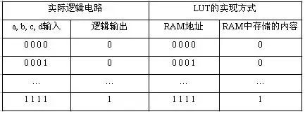 From this, we can see that LUT has the same functionality as a logic circuit. In fact, LUT has faster execution speed and larger scale. Due to the high integration of LUT-based FPGAs, their device density ranges from tens of thousands to tens of millions of gates, enabling them to perform extremely complex timing and combinational logic functions, making them suitable for high-speed, high-density high-end digital logic circuit design. Their components mainly include programmable input/output units, basic programmable logic units, embedded SRAM, rich routing resources, embedded functional units, and embedded dedicated units. Major design and production manufacturers include Xilinx, Altera, Lattice, Actel, Atmel, and QuickLogic, with Xilinx, Altera, and Lattice being the largest. As mentioned earlier, FPGAs are configured using RAM stored on the chip, so programming the internal RAM is required during operation. Users can adopt different programming methods based on different configuration modes. FPGA has the following configuration modes:
- Parallel mode: Configuring FPGA with parallel PROM or Flash;
- Master-slave mode: One PROM configures multiple FPGAs;
- Serial mode: Configuring FPGA with serial PROM;
- Peripheral mode: Using FPGA as a peripheral of a microprocessor, programmed by the microprocessor.
Currently, the two companies with the highest market share in FPGA, Xilinx and Altera, produce FPGAs based on SRAM technology, requiring an external memory chip to save the program during use. Upon power-up, the FPGA reads data from the external memory into the internal RAM, completes configuration, and enters operational status; after power-off, the FPGA returns to a blank state, losing internal logic. This allows FPGA to be reused without requiring a dedicated FPGA programmer, only a general EPROM or PROM programmer. Companies like Actel and QuickLogic also offer antifuse technology FPGAs, which can only be programmed once, providing advantages such as radiation resistance, high and low-temperature tolerance, low power consumption, and high speed, making them widely used in military and aerospace applications. However, these FPGAs cannot be reprogrammed, making initial development more complicated and costly. Lattice is the inventor of ISP technology, featuring certain characteristics in small-scale PLD applications. Early Xilinx products generally did not involve military and aerospace markets, but now several products like Q Pro-R have entered this field.FPGA Chip StructureCurrently, mainstream FPGAs are still based on LUT technology, far exceeding the basic performance of earlier versions, and integrating commonly used functions (such as RAM, clock management, and DSP) into hard-core (ASIC-type) modules. As shown in Figure 1-1 (note: Figure 1-1 is only a schematic; in reality, each series of FPGA has its corresponding internal structure), FPGA chips are mainly composed of six parts: programmable input/output units, basic programmable logic units, complete clock management, embedded block RAM, rich routing resources, embedded functional units, and embedded dedicated hardware modules.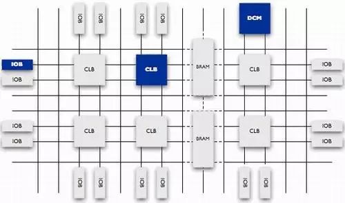 Figure 1-1 Internal Structure of FPGA ChipThe functions of each module are as follows:1. Programmable Input/Output Unit (IOB) The programmable input/output unit, referred to as I/O unit, is the interface between the chip and external circuits, fulfilling the driving and matching requirements for input/output signals under different electrical characteristics. Its schematic structure is shown in Figure 1-2. The I/Os in the FPGA are classified into groups, with each group independently supporting different I/O standards. Through flexible software configuration, they can adapt to various electrical standards and I/O physical characteristics, adjust driving current, and change pull-up and pull-down resistors. Currently, the frequency of I/O ports is also increasing, with some high-end FPGAs supporting data rates of up to 2Gbps through DDR register technology.
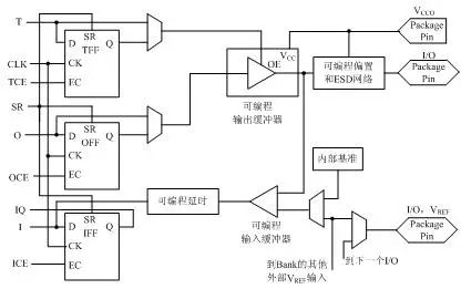 Figure 1-2 Schematic Diagram of Typical IOB Internal StructureExternal input signals can be input into the FPGA’s internal through the storage unit of the IOB module or directly into the FPGA. When external input signals are input into the FPGA through the storage unit of the IOB module, the hold time requirement can be reduced, usually defaulting to 0. To facilitate management and adapt to various electrical standards, the FPGA’s IOB is divided into several groups (banks), with the interface standard of each bank determined by its interface voltage VCCO. A bank can only have one VCCO, but different banks can have different VCCOs. Only ports with the same electrical standard can be connected together, and the same VCCO voltage is a basic condition for the interface standard.2. Configurable Logic Block (CLB) The CLB is the basic logic unit within the FPGA. The actual number and characteristics of CLBs vary depending on the device, but each CLB contains a configurable switch matrix, which consists of 4 or 6 inputs, some selection circuits (multiplexers, etc.), and flip-flops. The switch matrix is highly flexible and can be configured to handle combinational logic, shift registers, or RAM. In Xilinx’s FPGA devices, a CLB consists of multiple (generally 4 or 2) identical slices and additional logic, as shown in Figure 1-3. Each CLB module can be used to implement combinational logic, sequential logic, and can also be configured as distributed RAM and distributed ROM.
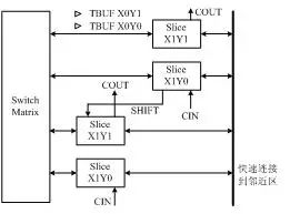 Figure 1-3 Schematic Diagram of Typical CLB StructureA slice is the basic logic unit defined by Xilinx, with its internal structure shown in Figure 1-4. A slice consists of two 4-input functions, carry logic, arithmetic logic, and function multiplexers. The arithmetic logic includes an XOR gate (XORG) and a dedicated AND gate (MULTAND), where an XOR gate allows a slice to perform 2-bit full addition, and the dedicated AND gate improves the efficiency of multipliers; the carry logic consists of dedicated carry signals and function multiplexers (MUXC) for implementing fast arithmetic addition and subtraction; the 4-input function generator is used to implement 4-input LUT, distributed RAM, or 16-bit shift registers (in the Virtex-5 series chips, the two input functions in the slice can be 6-input, allowing for 6-input LUT or 64-bit shift registers); the carry logic includes two fast carry chains to enhance the processing speed of the CLB module.
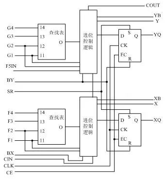 Figure 1-4 Schematic Diagram of Typical 4-Input Slice Structure3. Digital Clock Management Module (DCM) Most FPGAs in the industry provide digital clock management (all Xilinx FPGAs have this feature). Xilinx’s most advanced FPGAs offer digital clock management and phase-locked loops. Phase-locked loops can provide precise clock synthesis, reduce jitter, and achieve filtering functions.4. Embedded Block RAM (BRAM) Most FPGAs have embedded block RAM, greatly expanding the application range and flexibility of FPGAs. Block RAM can be configured as single-port RAM, dual-port RAM, content-addressable memory (CAM), and FIFO, among other common storage structures. RAM and FIFO are widely understood concepts, so they will not be elaborated here. CAM memory has a comparison logic in each storage unit, and data written into CAM will be compared with every internal data, returning the addresses of all data that match the port data, thus widely used in routing address switches. In practical applications, the number of internal block RAMs is also an important factor in selecting a chip. The capacity of a single block RAM is 18k bits, meaning a bit width of 18 bits and a depth of 1024, which can be adjusted as needed, but must meet two principles: first, the modified capacity (bit width x depth) cannot exceed 18k bits; second, the bit width cannot exceed 36 bits. Of course, multiple block RAMs can be cascaded to form larger RAM, in which case the only limitation is the number of block RAMs within the chip, no longer constrained by the above two principles.5. Rich Routing Resources Routing resources connect all units within the FPGA, and the length and technology of the connections determine the driving capability and transmission speed of signals on the connections. FPGA chips have abundant routing resources, classified into four different categories based on technology, length, width, and distribution. The first category is global routing resources, used for global clock and global reset/set routing within the chip; the second category is long-line resources, used for high-speed signals and secondary global clock signal routing between chip banks; the third category is short-line resources, used for logical interconnections and routing between basic logic units; the fourth category is distributed routing resources, used for dedicated clock, reset, and other control signal lines. In practice, designers do not need to directly select routing resources; the layout and routing tools automatically select routing resources to connect various module units based on the topology of the input logic netlist and constraints. Essentially, the method of using routing resources is closely and directly related to the design results.6. Embedded Functional Units The embedded functional modules mainly refer to soft processing cores (Soft Cores) such as DLL (Delay Locked Loop), PLL (Phase Locked Loop), DSP, and CPU. The increasingly rich embedded functional units make single-chip FPGAs system-level design tools, enabling them to possess the capability for hardware-software co-design, gradually transitioning to SOC platforms. DLL and PLL have similar functions, capable of achieving high-precision, low-jitter clock multiplication and division, as well as duty cycle adjustment and phase shifting. Chips produced by Xilinx integrate DLL, while Altera’s chips integrate PLL, and Lattice’s new chips integrate both PLL and DLL. DLL and PLL can be easily managed and configured using tools generated by IP cores. The structure of DLL is shown in Figure 1-5.
 Figure 1-5 Schematic Diagram of Typical DLL Module7. Embedded Dedicated Hard Cores Embedded dedicated hard cores refer to powerful hard cores (Hard Cores) within the FPGA, equivalent to ASIC circuits. To enhance FPGA performance, chip manufacturers integrate some dedicated hard cores within the chip. For example, to improve the speed of multiplication in FPGAs, mainstream FPGAs integrate dedicated multipliers; to accommodate communication bus and interface standards, many high-end FPGAs integrate serial/parallel transceivers (SERDES), achieving transceiving speeds of several tens of Gbps. Xilinx’s high-end products not only integrate Power PC series CPUs but also embed DSP Core modules, with corresponding system-level design tools being EDK and Platform Studio, thus proposing the concept of System on Chip (SoC). Through platforms like PowerPC, Microblaze, and Picoblaze, standard DSP processors and related applications can be developed to achieve SoC development goals.Concepts of Soft Cores, Hard Cores, and Firm CoresIP (Intelligent Property) cores refer to integrated circuit cores with intellectual property rights, which are verified macro modules with specific functions, independent of chip manufacturing processes, and can be ported to different semiconductor processes. At the SOC stage, IP core design has become an important task for ASIC circuit design companies and FPGA providers, reflecting their strength. The richer the IP cores provided by FPGA development software, the more convenient the design for users, leading to higher market share. Currently, IP cores have become the basic unit of system design and are exchanged, transferred, and sold as independent design achievements. Based on the way IP cores are provided, they are typically divided into three categories: soft cores, hard cores, and firm cores. In terms of the cost incurred to complete the IP core, hard cores are the most expensive; in terms of flexibility of use, soft cores have the highest reusability.1. Soft Cores Soft cores in the EDA design field refer to register transfer level (RTL) models before synthesis; specifically, in FPGA design, they refer to hardware language descriptions of circuits, including logic descriptions, netlists, and help documents. Soft cores only undergo functional simulation and require synthesis and layout routing before use. Their advantages include high flexibility and strong portability, allowing user configuration; however, they have lower predictability for modules, posing a risk of errors in subsequent designs. Soft cores are the most widely used form of IP cores.2. Firm Cores Firm cores in the EDA design field refer to netlists with planar layout information; specifically, in FPGA design, they can be seen as soft cores with layout planning, usually provided in a mixed form of RTL code and corresponding specific process netlists. By combining RTL descriptions with specific standard cell libraries for synthesis optimization, a gate-level netlist is formed, which can be used through layout and routing tools. Compared to soft cores, firm cores have slightly lower design flexibility but significantly improved reliability. Currently, firm cores are also one of the mainstream forms of IP cores.3. Hard Cores Hard cores in the EDA design field refer to verified design layouts; specifically, in FPGA design, they refer to designs with fixed layouts and processes that have been verified in both front-end and back-end, which designers cannot modify. The reasons for the inability to modify are twofold: first, the system design has strict timing requirements for each module, not allowing disruption of the existing physical layout; second, protecting intellectual property rights requires that designers cannot make any changes. The unmodifiable characteristic of IP hard cores makes their reuse somewhat difficult, thus limiting their application to specific uses with a narrower range.