Semiconductor materials are a class of materials that possess semiconductor properties (the conductivity is between that of conductors and insulators, with resistivity ranging from approximately 1 mΩ·cm to 1 GΩ·cm). Generally, the conductivity increases with rising temperature.
Semiconductor materials have characteristics such as thermal sensitivity, optical sensitivity, and doping capability. They are important materials used in wafer manufacturing and backend packaging, widely applied in integrated circuits or various semiconductor devices in fields like automotive, lighting, home appliances, consumer electronics, and information communications.
Moreover, semiconductor materials and devices are the foundation of the semiconductor industry chain and serve as the driving force behind innovation in integrated circuit technology. Wafer fabs must purchase equipment and materials and acquire corresponding process technologies to operate normally. On the other hand, the three are interdependent; improvements in materials often require simultaneous updates in equipment and processes to effectively avoid the ‘barrel effect’.
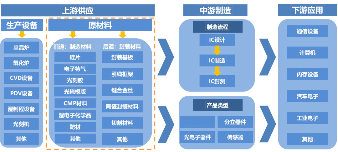
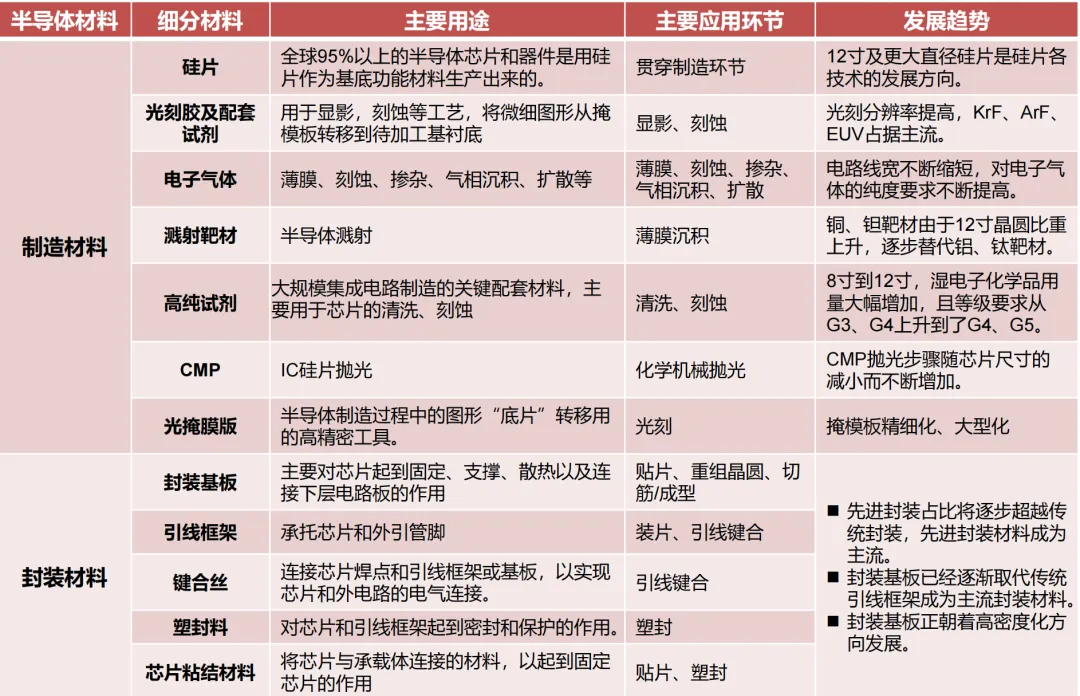
Semiconductor materials are located upstream in the industry chain and come in a wide variety. Each individual process in chip manufacturing is paired with corresponding materials. Based on application stages, semiconductor materials are mainly divided into manufacturing materials and packaging materials.
The main manufacturing materials include wafers (silicon-based materials), photoresists and supporting reagents, high-purity reagents, electronic gases, polishing materials, target materials, and masks; the main packaging materials include lead frames, packaging substrates, ceramic substrates, bonding wires, packaging materials, and chip adhesive materials.
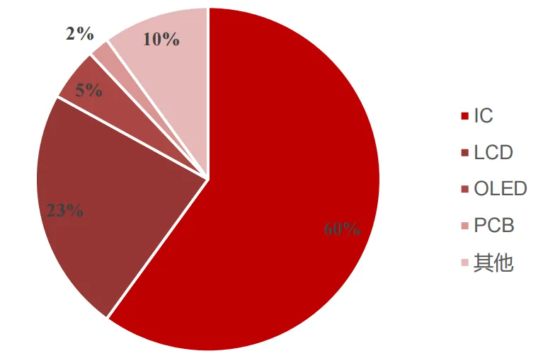
The main segmented uses and application stages of semiconductor materials run through manufacturing and testing.
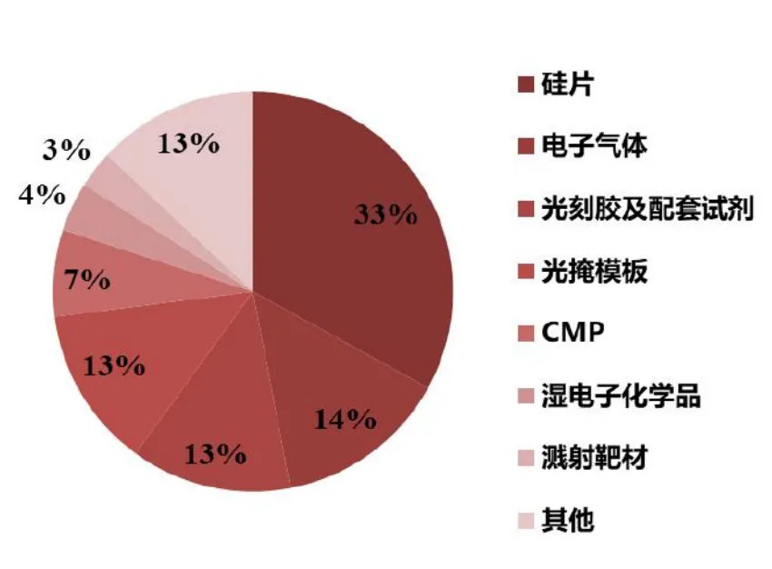
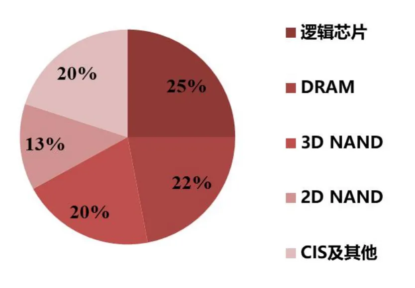
The upgrade of chip manufacturing technologies and the expansion of wafer fabs are significantly driving the increase in China’s chip shipments, which raises higher demands for the consumption and quality of semiconductor materials. In the future, the domestic production rate will steadily increase. Among semiconductor manufacturing materials, wafers account for the largest share (approximately 33%), followed by gases and photoresists along with supporting reagents.
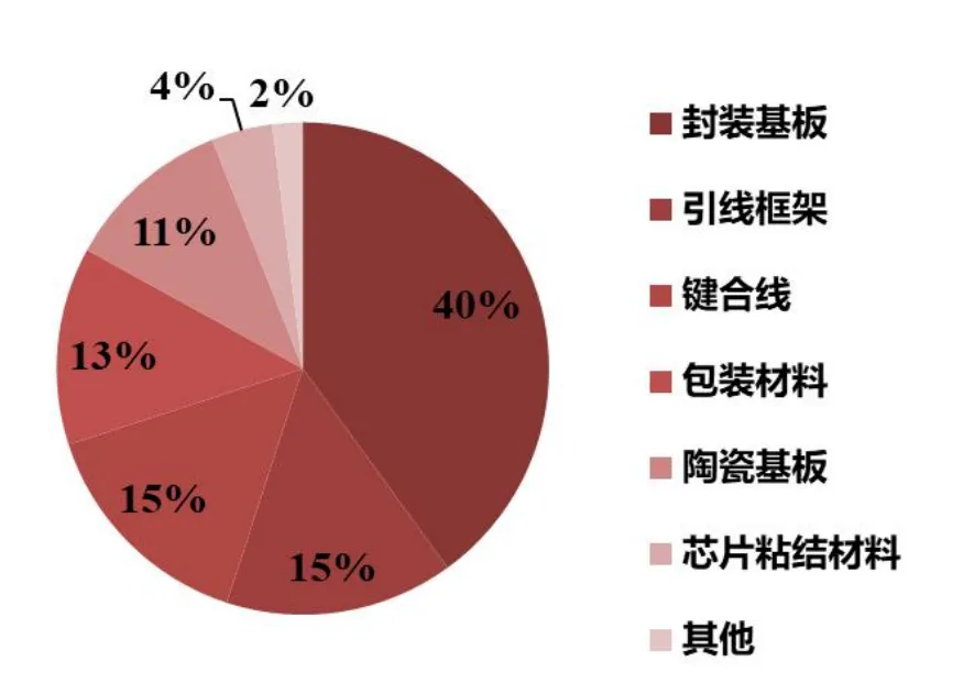
In semiconductor packaging materials, packaging substrates hold the largest share (approximately 40%), followed by lead frames and bonding wires. Overall, each segmented semiconductor materials market is generally quite small.
There are numerous subdivisions in semiconductor materials, making it the segment of the industry chain with the most subdivisions. Each major category of materials includes dozens or even hundreds of specific products, with the number of segmented sub-industries reaching into the hundreds. For example, common high-purity chemical reagents include various acids (such as sulfuric acid, hydrochloric acid, nitric acid, phosphoric acid), bases (such as ammonium hydroxide, potassium hydroxide), organic solvents, and oxidizing agents. Considering the industry characteristics of semiconductor materials, we believe that semiconductor material companies should actively look for commonalities among various materials, continuously expand their categories, and form a platform layout to provide integrated solutions for customers.
Currently, the mainstream products in the global market are semiconductor silicon wafers with diameters of 200mm (8 inches) and 300mm (12 inches). The investment in equipment in the downstream chip manufacturing industry is also matched with the specifications of 200mm and 300mm. The 300mm chip manufacturing corresponds to process technologies of 90nm and below, while 200mm chip manufacturing corresponds to process technologies above 90nm. Considering that most 8-inch wafer production lines have been in operation for a longer time, the vast majority of equipment has been fully depreciated. Therefore, the chip cost corresponding to 8-inch wafers is relatively low, and in some fields, the comprehensive cost of using 8-inch wafers is not higher than that of 12-inch wafers.
In terms of high-precision analog circuits, RF front-end chips, embedded memory, CMOS image sensors, and high-voltage MOS, the manufacturing process for chips of 200mm and below is more mature than that for 12-inch wafers. Thus, the demand for 200mm and below semiconductor silicon wafers mainly comes from power devices, power management devices, non-volatile memory, MEMS, display driver chips, and fingerprint recognition chips. The terminal application fields mainly include mobile communications, automotive electronics, the Internet of Things, and industrial electronics.
Currently, the demand for 300mm (12-inch) semiconductor silicon wafers mainly comes from memory chips, image processing chips, general-purpose processor chips, high-performance FPGAs, and ASICs, with terminal applications primarily in high-end fields such as smartphones, computers, cloud computing, artificial intelligence, and SSDs.
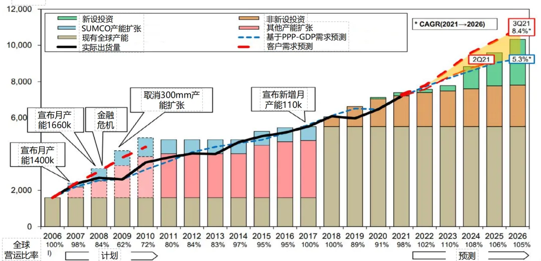
According to announcements from XinYue Chemical, global semiconductor silicon wafer shipments have been growing year-on-year and quarter-on-quarter, with nearly all silicon wafer suppliers operating at high capacity. The new demand for 12-inch wafers mainly comes from logic epitaxial wafers, while 8-inch wafers are in severe shortage due to downstream applications (such as automotive electronics) and global economic recovery.
According to SUMCO’s announcement, the spot price of semiconductor silicon wafers continued to rise in Q4 2021, and long-term contract prices for semiconductor silicon wafers from 2022 to 2026 will increase. We believe that the global silicon wafer shortage will last at least until the end of 2023.
The Chinese semiconductor silicon wafer industry chain involves the manufacturing of electronic-grade polysilicon, semiconductor silicon wafer manufacturing, and semiconductor device manufacturing. The main participants are semiconductor silicon wafer manufacturers, integrated semiconductor industry chain manufacturers, and semiconductor material manufacturers with diversified layouts.
Currently, in the upstream raw material sector, electronic-grade polysilicon mainly relies on imports, with only a few companies capable of mass production; in the midstream semiconductor silicon wafer manufacturing sector, companies like Zhonghuan Semiconductor, Shanghai Silicon Industry, and Lian Microelectronics have achieved mass production of 8-inch and 12-inch wafers; in the downstream semiconductor manufacturing sector, SMIC, Hua Hong Semiconductor, and China Resources Microelectronics have begun domestic substitution.
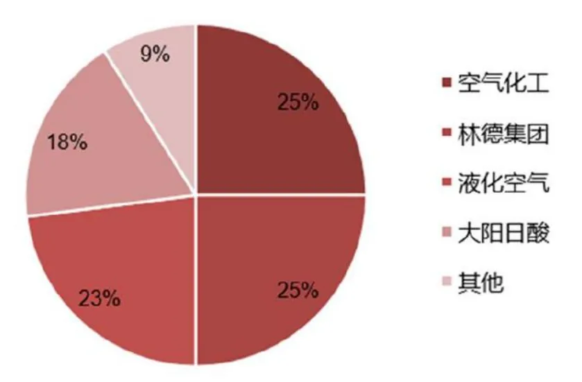
According to Techcet data, the global electronic gas market size is expected to exceed $8 billion by 2025, with an annual compound growth rate of 6.5%. The global specialty gas market size is expected to exceed $6 billion by 2025, with an annual compound growth rate of approximately 7.5%.
The domestic production level of electronic gases is relatively high. Domestic electronic gas suppliers include Jin Hong Gas, Huate Gas, and China Shipbuilding Industry Corporation. China Shipbuilding is known for its trifluoride nitrogen and hexafluoride tungsten; Jin Hong Gas is a leading domestic specialty gas company providing liquid carbon dioxide, ultra-pure ammonia, etc.; Huate Gas is the only domestic company certified for ASML lithography gases, mainly including some neon-containing specialty gases.
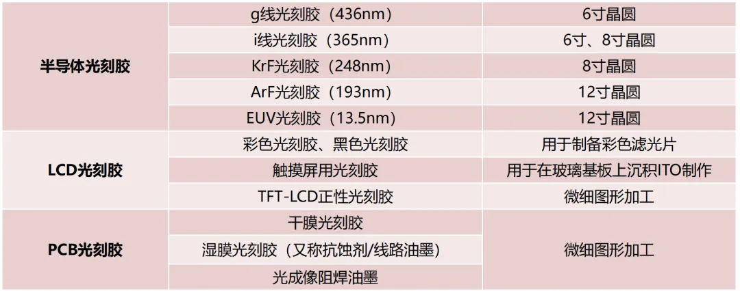
In terms of photoresists, after decades of continuous development and progress, the application fields have continuously expanded, leading to the derivation of many types. Based on application fields, photoresists can be divided into semiconductor photoresists, flat panel display photoresists, and PCB photoresists, with corresponding technical barriers decreasing in order. Accordingly, PCB photoresists are currently progressing the fastest in domestic substitution, LCD photoresists are relatively fast, while semiconductor photoresists currently lag the most behind foreign advanced technologies.
-
Based on the chemical reaction mechanism, photoresists can be divided into negative photoresists and positive photoresists.
-
Based on the chemical structure of raw materials, photoresists can be divided into photopolymerizable resins, photodecomposable resins, and photo-crosslinkable resins.
The global competitive landscape of photoresists: the photoresist market is mainly dominated by companies from Japan, the US, and South Korea, with mainland companies holding less than 10% market share. Among them, Japanese companies firmly hold the leading position in the global semiconductor photoresist market, occupying at least 60% share.
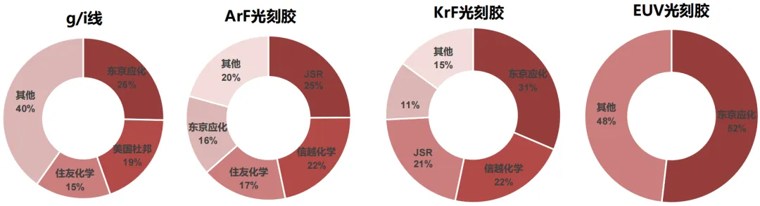
In the global semiconductor photoresist market, Japanese companies firmly hold the leading position. We estimate that the domestic substitution rate for g/i line photoresists is about 20%, while the KrF photoresists are below 5%, and the ArF photoresists are almost entirely dependent on imports. High-end photoresists are long-term monopolized by foreign companies, posing a risk of bottleneck for Chinese chip manufacturing.
Due to the short shelf life of high-end photoresists (usually only about 6 months or even shorter), in the event of trade conflicts or natural disasters, the Chinese integrated circuit industry is likely to face severe adverse situations with chip companies halting production altogether in the short term.
A mask is a graphic template used in the lithography process of microelectronics manufacturing. The global market for semiconductor photomasks continues to grow. Benefiting from the rapid development of wafer manufacturing in mainland China over the past few years, the semiconductor chip photomask market in mainland China has shown a trend of rapid growth.
Additionally, the photomask market has a high concentration, primarily dominated by foreign companies. Photronics, Japan’s DNP, and Japan’s Toppan together occupy over 80% of the semiconductor photomask market share. The Chinese photomask industry can only meet the domestic demand for mid- to low-end products.
This article is from: Founder Securities.
How to Let More People Know About Your Academic Achievements and Products?
Practical! Classic Problems Collection for Origin Software Use
Free Download:18 Extremely Useful Software for Easy Research
Cooperation Submission Click Here
Welcome to leave comments and share your views. Light up to see