Electronics Association Maker Lab
SPI stands for Serial Peripheral Interface. It is a high-speed, full-duplex, synchronous communication bus widely used in communication with ADCs, LCDs, and other devices connected to MCUs, characterized by its speed.

SPI Protocol
Like IIC and serial ports, SPI also has its communication protocol, which is generally learned in a layered manner, mainly divided into physical layer and protocol layer.
·Physical Layer
The common connection method between SPI communication devices consists of three buses and a chip select line between the master and slave:
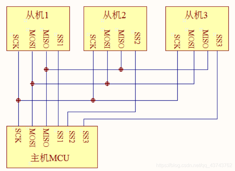
NSS: Chip select line, each slave has its own separate bus connected to the master, this bus is used for the master to select the corresponding slave for data transmission, and the NSS bus between each slave and the master is independent. SPI specifies that communication starts with the NSS signal line pulled low and ends when pulled high.
SCK: Clock signal line, because SPI is synchronous communication, a clock signal line is needed to unify the data transmission between the master and slave; data can only be transmitted normally under an effective clock signal. The maximum transmission frequency supported by different devices may vary, and during transmission, the transmission frequency is limited by the slower device.
MOSI: (Master Output, Slave Input), as the name suggests, MOSI is the master output/slave input. Since SPI is a full-duplex communication bus, the master and slave can send and receive data simultaneously, which requires two lines to be responsible for the two transmission paths: master -> slave and slave -> master. MOSI specifically handles data transmission from the master to the slave.
MISO: (Master Input, Slave Output), conversely, MISO is responsible for data transmission from the slave to the master.
·Protocol Layer
Similar to IIC, the SPI protocol layer specifies the start signal, stop signal, data validity, clock synchronization, and communication modes during the transmission process.
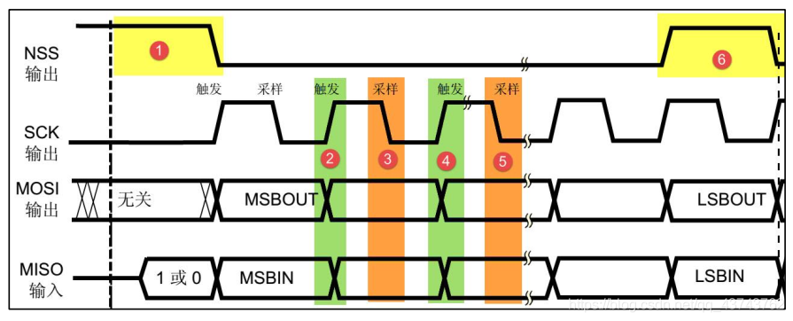
·Communication Timing Diagram
Below is a timing diagram for one of the communication modes of SPI:
·Start and Stop Signals
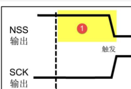
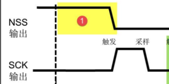
The start and stop of SPI communication are controlled by the NSS signal line. When NSS is low, it represents the start signal; when NSS is high, it represents the stop signal. The sections 1 and 6 in the timing diagram represent the start and stop signals.
·Data Validity
In SPI, full-duplex data transmission is performed using MOSI and MISO, with SCK synchronizing the data transmission. This means that MOSI and MISO work simultaneously, and data is sampled when the clock signal line SCK is valid. The sampled information is the transmitted information. In IIC communication, data is sampled when the SCL bus is high, while in SPI, data is sampled on the rising or falling edge of SCK. In the illustrated mode, sections 3 and 5 represent the moments of data sampling, showing that data is sampled on the falling edge of SCK. The high and low levels of MOSI and MISO represent 1 and 0.
·Communication Modes
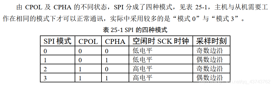
SPI has four communication modes, distinguished mainly by the clock state when the bus is idle and the timing of data sampling. This involves knowledge of clock polarity CPOL and clock phase CPHA.
Clock Polarity CPOL: CPOL refers to the level signal of SCK when the NSS bus is idle. If SCK is high, CPOL=1; if SCK is low, CPOL=0. In the below case, CPOL=0.
Clock Phase CPHA: CPHA refers to the sampling moment of the data. The SCK signal can be viewed as a square wave. When CPHA=0, data is sampled on the odd edges of SCK; when CPHA=1, data is sampled on the even edges of SCK.
As shown: When NSS is idle, SCK is low, and data is sampled on the falling edge of SCK (the second edge), so in this communication mode, CPOL=0, CPHA=1.
Four Communication Modes: Based on the combinations of CPOL and CPHA, four different communication modes can be derived, as follows:
SPI in STM32
STM32 integrates peripherals specifically for SPI communication. The maximum SCK clock frequency supported is fpclk/2
(For STM32F103 models, the default fpclk1 is 72MHz, and fpclk2 is 36MHz), fully supporting the four modes of the SPI protocol, with the data frame length settable to 8 or 16 bits, and the data can be configured to be MSB first or LSB first. It also supports dual-line full-duplex, dual-line unidirectional, and single-line modes. The dual-line unidirectional mode can use both MOSI and MISO data lines to transmit data in one direction, effectively doubling the transmission speed. The single-line mode reduces hardware wiring, although the speed is affected.
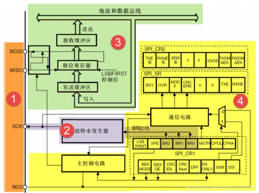
The functional block diagram is as follows:
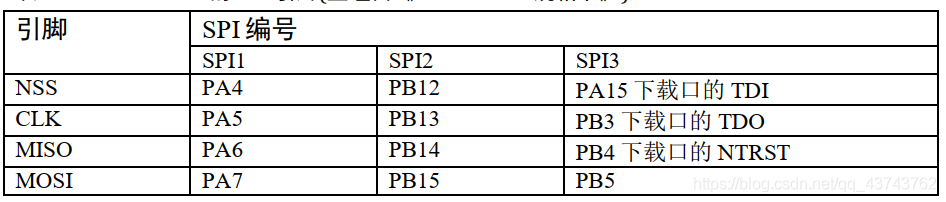
·Communication Pins
STM32 has multiple SPI peripherals, and the MOSI, MISO, SCK, NSS pins all correspond to specific pins. When using the respective SPI, these corresponding pins must be configured. The pin distribution of the three SPI peripherals in STM32 is as follows:
·Clock Control Logic
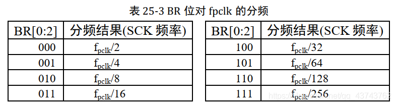
The baud rate generator configures the frequency division factor of fpclk through the three bits BR[2:0] in the “Control Register CR1”. The frequency after dividing fpclk is the clock frequency of SCK, as shown in the following configuration (fpclk is the clock frequency corresponding to the SPI mounting bus):
Configuration of Communication Modes: The communication mode can be configured as one of the four modes mentioned above by setting the CPOL and CPHA bits in the “Control Register CR”.
·Data Control Logic
This part mainly controls data reception and transmission, as well as data frame format and MSB/LSB precedence, similar to serial communication. SPI’s data transmission and reception are also achieved through buffers and shift registers.
MOSI and MISO are both connected to the shift register for data transmission.
Sending Data: The address and data bus will fetch the data to be sent at the corresponding address, placing the data into the transmit buffer. When sending data out, the shift register will use the transmit buffer as the data source, sending the data out one bit at a time.
Receiving Data: During data reception, the shift register samples the data from the data line one bit at a time and transfers it to the receive buffer, which can then be read from the bus.
Data Frame Format: The data frame format can be controlled to be 8 bits or 16 bits by configuring the “DFF bit” in the “Control Register CR1”, which determines the size of data received or sent at one time.
Precedence Bit: The “LSBFIRST bit” in the “Control Register CR1” can be configured to choose either MSB (Most Significant Bit) first or LSB (Least Significant Bit) first.
·Overall Logic Control
During peripheral operation, the control logic modifies the “Status Register (SR)” based on the working state of the peripheral. By reading the relevant bits in the status register, one can understand the working state of SPI.
Additionally, the control logic is responsible for generating SPI interrupt signals, DMA requests, and controlling the NSS signal line. However, the NSS signal line is generally connected to GPIO ports, controlled by software to produce the start and stop signals.
Initialization Structure for SPI Peripheral
typedef struct { uint16_t SPI_Direction; /* Set SPI's unidirectional or bidirectional mode */ uint16_t SPI_Mode; /* Set SPI's master/slave mode */ uint16_t SPI_DataSize; /* Set SPI's data frame length, options 8/16 bits */ uint16_t SPI_CPOL; /* Set clock polarity CPOL, options high/low level */ uint16_t SPI_CPHA; /* Set clock phase, options odd/even edge sampling */ uint16_t SPI_NSS; /* Set NSS pin controlled by SPI hardware or software */ uint16_t SPI_BaudRatePrescaler; /* Set clock division factor, fpclk/divider=fSCK */ uint16_t SPI_FirstBit; /* Set MSB/LSB precedence */ uint16_t SPI_CRCPolynomial; /* Set CRC check expression */ } SPI_InitTypeDef;(1)SPI_Direction
This member sets the communication direction of SPI, which can be set to dual-line full-duplex (SPI_Direction_2Lines_FullDuplex), dual-line receive only (SPI_Direction_2Lines_RxOnly), single-line receive only (SPI_Direction_1Line_Rx), or single-line transmit only (SPI_Direction_1Line_Tx).
(2) SPI_Mode
This member sets SPI to operate in master mode (SPI_Mode_Master) or slave mode (SPI_Mode_Slave). The main difference between these two modes is the timing of the SCK signal line, which is generated by the master during communication. If configured in slave mode, the STM32 SPI peripheral will accept external SCK signals.
(3) SPI_DataSize
This member can choose the size of the SPI communication data frame to be either 8 bits (SPI_DataSize_8b) or 16 bits (SPI_DataSize_16b).
(4)SPI_CPOL and SPI_CPHA
These two members configure the clock polarity CPOL and clock phase CPHA of SPI communication, affecting the communication modes. The clock polarity CPOL member can be set to high level (SPI_CPOL_High) or low level (SPI_CPOL_Low). The clock phase CPHA can be set to SPI_CPHA_1Edge (sampling data on the odd edge of SCK) or SPI_CPHA_2Edge (sampling data on the even edge of SCK).
(5)SPI_NSS
This member configures the usage mode of the NSS pin, which can be set to hardware mode (SPI_NSS_Hard) or software mode (SPI_NSS_Soft). In hardware mode, the SPI chip select signal is automatically generated by the SPI hardware, while in software mode, we manually pull the corresponding GPIO port high or low to generate non-chip select and chip select signals. Software mode is more commonly used in practice.
(6) SPI_BaudRatePrescaler
This member sets the baud rate division factor, and the clock after division is the clock frequency of the SPI’s SCK signal line. This member parameter can be set to 2, 4, 6, 8, 16, 32, 64, 128, or 256 division of fpclk.
(7) SPI_FirstBit
All serial communication protocols will have the issue of MSB precedence (most significant bit first) or LSB precedence (least significant bit first), and the STM32 SPI module can programmatically control this feature through this structure member.
(8) SPI_CRCPolynomial
This is the polynomial for CRC check in SPI. If we use CRC checks, we will use the parameter (polynomial) of this member to calculate the CRC value.
Initial Configuration Function
void SPI_Config(void){ /* Initialize SPI and corresponding GPIO ports */ SPI_InitTypeDef SPI_InitStruct; GPIO_InitTypeDef GPIO_InitStruct; /* Enable clock for SPI1 and GPIOA */ RCC_APB2PeriphClockCmd(RCC_APB2Periph_SPI1 | RCC_APB2Periph_GPIOA, ENABLE); /* Configure NSS as normal push-pull mode, SCK, MISO, MOSI as multiplexed push-pull mode */ GPIO_InitStruct.GPIO_Mode = SPI_SCK_GPIO_MODE; GPIO_InitStruct.GPIO_Pin = SPI_SCK_GPIO_PIN; GPIO_InitStruct.GPIO_Speed = SPI_SCK_GPIO_SPEED; GPIO_Init(SPI_SCK_GPIO_PORT, &GPIO_InitStruct); GPIO_InitStruct.GPIO_Mode = SPI_MOSI_GPIO_MODE; GPIO_InitStruct.GPIO_Pin = SPI_MOSI_GPIO_PIN; GPIO_InitStruct.GPIO_Speed = SPI_MOSI_GPIO_SPEED; GPIO_Init(SPI_MOSI_GPIO_PORT, &GPIO_InitStruct); GPIO_InitStruct.GPIO_Mode = SPI_MISO_GPIO_MODE; GPIO_InitStruct.GPIO_Pin = SPI_MISO_GPIO_PIN; GPIO_InitStruct.GPIO_Speed = SPI_MISO_GPIO_SPEED; GPIO_Init(SPI_MISO_GPIO_PORT, &GPIO_InitStruct); GPIO_InitStruct.GPIO_Mode = SPI_NSS_GPIO_MODE; GPIO_InitStruct.GPIO_Pin = SPI_NSS_GPIO_PIN; GPIO_InitStruct.GPIO_Speed = SPI_NSS_GPIO_SPEED; GPIO_Init(SPI_NSS_GPIO_PORT, &GPIO_InitStruct); /* Configure SPI for 4 division, SCK idle high, even edge sampling, 8-bit data frame, MSB first, software NSS, dual-line full-duplex mode, SPI peripheral as master */ SPI_InitStruct.SPI_BaudRatePrescaler = SPIx_BaudRatePrescaler; SPI_InitStruct.SPI_CPHA = SPIx_CPHA; SPI_InitStruct.SPI_CPOL = SPIx_CPOL; SPI_InitStruct.SPI_CRCPolynomial = SPIx_CRCPolynomial; SPI_InitStruct.SPI_DataSize = SPIx_DataSize; SPI_InitStruct.SPI_Direction = SPIx_Direction; SPI_InitStruct.SPI_FirstBit = SPIx_FirstBit; SPI_InitStruct.SPI_Mode = SPIx_Mode; SPI_InitStruct.SPI_NSS = SPIx_NSS; /* Write SPI peripheral configuration information to registers and enable SPI peripheral */ SPI_Init(SPIx, &SPI_InitStruct); SPI_Cmd(SPIx, ENABLE); /* Pull NSS high */ SPI_NSS_Stop();} }Send and Receive One Byte
/* Send a frame of data, simultaneously receive a frame of data */uint8_t SPI_SendData( uint8_t data){ uint16_t timeout=0x2710; //10,000 while(SPI_I2S_GetFlagStatus(SPIx, SPI_I2S_FLAG_TXE)==RESET) // Register status can be read at any time, not influenced by whether SPI is transmitting data if((timeout--)==0) return printf("Send wait failed!\n"); SPI_I2S_SendData(SPIx, data); timeout=0x2710; //10,000 cycles without result means failure while(SPI_I2S_GetFlagStatus(SPIx, SPI_I2S_FLAG_RXNE)==RESET) if((timeout--)==0) return printf("Receive wait failed!\n"); return SPI_I2S_ReceiveData(SPIx);}/* Read a frame of data */uint16_t SPI_ReadData(void){ return SPI_SendData( 1);// The value sent can be arbitrary}Header File
#ifndef __SPI_H#define __SPI_H#include "stm32f10x.h"#define SPIx SPI1#define SPI_Clock RCC_APB2Periph_SPI1#define SPI_GPIO_Clock RCC_APB2Periph_GPIOA/* SCK/MOSI/MISO configured as multiplexed push-pull output, NSS controlled by software configured as normal push-pull output */#define SPI_SCK_GPIO_PORT GPIOA#define SPI_SCK_GPIO_MODE GPIO_Mode_AF_PP#define SPI_SCK_GPIO_SPEED GPIO_Speed_50MHz#define SPI_SCK_GPIO_PIN GPIO_Pin_5#define SPI_MOSI_GPIO_PORT GPIOA#define SPI_MOSI_GPIO_MODE GPIO_Mode_AF_PP#define SPI_MOSI_GPIO_SPEED GPIO_Speed_50MHz#define SPI_MOSI_GPIO_PIN GPIO_Pin_7#define SPI_MISO_GPIO_PORT GPIOA#define SPI_MISO_GPIO_MODE GPIO_Mode_AF_PP#define SPI_MISO_GPIO_SPEED GPIO_Speed_50MHz#define SPI_MISO_GPIO_PIN GPIO_Pin_6#define SPI_NSS_GPIO_PORT GPIOA#define SPI_NSS_GPIO_MODE GPIO_Mode_Out_PP#define SPI_NSS_GPIO_SPEED GPIO_Speed_50MHz#define SPI_NSS_GPIO_PIN GPIO_Pin_4 // Because the serial FLASH's CS pin is PA4, SPI's NSS should be consistent with it/* Configure SPI information */#define SPIx_BaudRatePrescaler SPI_BaudRatePrescaler_4// Four division, SPI1 mounted on APB2, baud rate after four division is 18MHz#define SPIx_CPHA SPI_CPHA_2Edge// Even edge sampling#define SPIx_CPOL SPI_CPOL_High// SCK high level when idle#define SPIx_CRCPolynomial 7// Not using CRC function, so it does not matter#define SPIx_DataSize SPI_DataSize_8b// Data frame format is 8 bits#define SPIx_Direction SPI_Direction_2Lines_FullDuplex#define SPIx_FirstBit SPI_FirstBit_MSB// MSB first#define SPIx_Mode SPI_Mode_Master// Master mode#define SPIx_NSS SPI_NSS_Soft// Software mode/***************************************************************************************/#define SPI_NSS_Begin() GPIO_ResetBits(SPI_NSS_GPIO_PORT, SPI_NSS_GPIO_PIN)#define SPI_NSS_Stop() GPIO_SetBits(SPI_NSS_GPIO_PORT, SPI_NSS_GPIO_PIN)#endif /*__SPI_H*/END

Electronics Association Maker Lab

Text and Image Editor: Yu Haiyan
Reviewers: Zeng Jiahao
Wu Chengyun
Chen Zhengfu