Introduction
The previous article detailed the SPI module under the Autosar architecture diagram, but did not cover the SPI communication bus. This article is a repost of what I consider to be a well-written introduction to the SPI communication protocol for your reference.
Reference Articles:
AUTOSAR-MCAL–Detailed Explanation of SPI Module (I)
AUTOSAR-MCAL–Detailed Explanation of SPI Module (II)
AUTOSAR-MCAL–Detailed Explanation of SPI Module (III)
Note: This article is reprinted from CSDN and organized by the WeChat public account “Ten Thousand Whys of Hardware”.
Main Text
1. Introduction to SPI
SPI, short for Serial Peripheral Interface, is a serial communication interface defined first by Motorola in its MC68HCXX series processors. The SPI interface is mainly used between EEPROM, FLASH, real-time clocks, AD converters, digital signal processors, and digital signal decoders. SPI is a high-speed, full-duplex, synchronous communication bus that only occupies four lines on the chip pins, saving chip pins and providing convenience for PCB layout. Due to its simple and easy-to-use characteristics, more and more chips are integrating this communication protocol.
2. Features of SPI
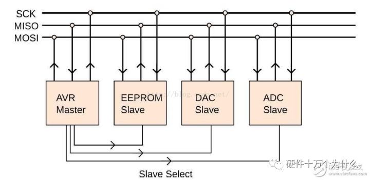
2.1 Master-Slave Control Mode
SPI stipulates that communication between two SPI devices must be controlled by a master device. A master device can control multiple slave devices by providing a clock and performing slave selection (Slave Select). The SPI protocol also specifies that the clock for the slave device is provided by the master device through the SCK pin, and the slave device itself cannot generate or control the clock. Without a clock, the slave device cannot function properly.
2.2 Synchronous Data Transmission
The master device generates corresponding clock pulses based on the data to be exchanged. These clock pulses form the clock signal, which controls when data is exchanged between the two SPI devices and when the received data is sampled, ensuring that data is transmitted synchronously between the two devices.
2.3 Data Exchange
The data transmission between SPI devices is referred to as data exchange because the SPI protocol stipulates that a SPI device cannot act solely as a transmitter or receiver during data communication. In each clock cycle, SPI devices send and receive a bit of data, meaning that one bit of data is exchanged. A slave device must be accessed by the master device before it can receive control signals from the master. Therefore, the master device must first select the desired slave device through the SS/CS pin. During data transmission, each received data must be sampled before the next data transmission. If the previously received data is not read, it may be discarded, causing the SPI physical module to fail. Therefore, it is common in programs to read the data from the SPI device after the SPI transmission is complete, even if this data (Dummy Data) is useless in our program.
2.4 Four Transmission Modes of SPI
There are rising edge, falling edge, leading edge, and trailing edge triggers. There are also MSB and LSB transmission methods.
2.5 Only Master and Slave Modes
There is no distinction between read and write, because essentially each SPI transaction involves the master and slave exchanging data. In other words, sending data will inevitably result in receiving data; to receive data, one must first send data.
3. Working Mechanism
3.1 Overview
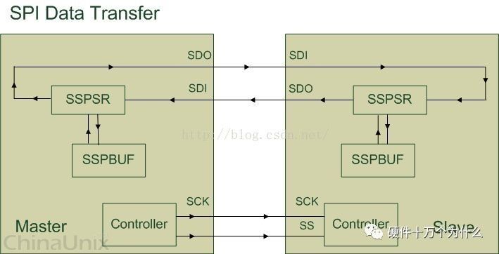
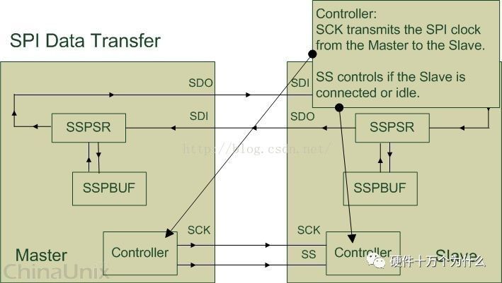
The above image provides a simple description of communication between SPI devices. Below, I will explain the components shown in the image:
SSPBUF, Synchronous Serial Port Buffer, refers to the internal buffer in SPI devices, typically in the form of FIFO, which stores temporary data during transmission;
SSPSR, Synchronous Serial Port Register, refers to the shift register in SPI devices, which shifts data into or out of SSPBUF based on the configured data bit width (bit-width);
Controller, refers to the control registers in SPI devices, which can be configured to set the transmission mode of the SPI bus. Usually, we only need to program the four pins described in the image to control data communication between SPI devices:
SCK, Serial Clock, primarily transmits clock signals from the master device to the slave device, controlling the timing and rate of data exchange;
SS/CS, Slave Select/Chip Select, is used by the master device to select the slave device, allowing the selected slave device to be accessed by the master;
SDO/MOSI, Serial Data Output/Master Out Slave In, also known as Tx-Channel on the master, serves as the data output for SPI devices;
SDI/MISO, Serial Data Input/Master In Slave Out, also known as Rx-Channel on the master, serves as the data input for SPI devices;
During communication, a data loop is formed between the master and slave devices, as shown in the image, using the SDO and SDI pins. SSPSR controls the data movement in and out of SSPBUF, while the controller determines the communication mode of the SPI bus, and SCK transmits the clock signal.
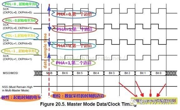
3.2 Timing
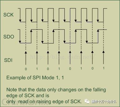
The above image illustrates the working mechanism of the SPI protocol by exchanging 1 Byte of data between the master and slave devices.
First, let’s explain the concepts of phase and polarity.
3.2.1 SPI Related Abbreviations or Terms
The polarity and phase of SPI are commonly denoted as CPOL and CPHA, but there are other notations as well. Here’s a simple summary:
(1) CKPOL (Clock Polarity) = CPOL = POL = Polarity = (Clock) Polarity
(2) CKPHA (Clock Phase) = CPHA = PHA = Phase = (Clock) Phase
(3) SCK=SCLK=SPI Clock
(4) Edge = The moment of clock level change, either rising edge or falling edge
For one clock cycle, there are two edges, referred to as: Leading edge = the first edge; if the starting voltage is 1, it is when it changes from 1 to 0; if the starting voltage is 0, it is when it changes from 0 to 1;
Trailing edge = the second edge; if the starting voltage is 1, it is when it changes from 0 to 1 (i.e., after the first 1 changes to 0, the subsequent 0 can change to 1); if the starting voltage is 0, it is when it changes from 1 to 0;
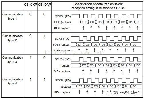
3.2.2 SPI Phase and Polarity
CPOL and CPHA can each be 0 or 1, resulting in four combinations: Mode 0 CPOL=0, CPHA=0; Mode 1 CPOL=0, CPHA=1; Mode 2 CPOL=1, CPHA=0; Mode 3 CPOL=1, CPHA=1.
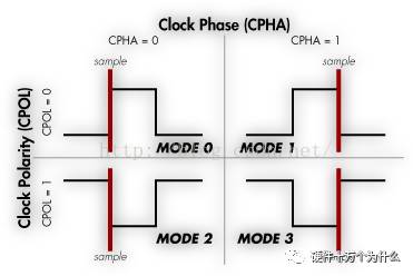
3.2.3 CPOL Polarity
Let’s first explain what the idle state of the SCLK clock is, which is the state before and after SCLK sends 8 bits of data. During data transmission, SCLK is in its active state.
In brief, Clock Polarity = IDLE state of SCK. To elaborate:
CPOL indicates whether the idle state of SCLK is low (0) or high (1):
CPOL=0 means the idle state is low, so when SCLK is active, it is high, which is called active-high;
CPOL=1 means the idle state is high, so when SCLK is active, it is low, which is called active-low;
3.2.4 CPHA Phase
First, it should be noted that capture strobe = latch = read = sample, all refer to data sampling, the moment when data is valid. The phase corresponds to which edge (first or second) the data is sampled at; 0 corresponds to the first edge, and 1 corresponds to the second edge.
For:
CPHA=0 indicates the first edge:
For CPOL=0 (idle is low), the first edge is from low to high (rising edge);
For CPOL=1 (idle is high), the first edge is from high to low (falling edge);
CPHA=1 indicates the second edge:
For CPOL=0 (idle is low), the second edge is from high to low (falling edge);
For CPOL=1 (idle is high), the second edge is from low to high (rising edge); the above image helps with understanding.
3.2.5 Setting SPI Polarity and Phase in Software
SPI consists of master and slave devices that communicate via the SPI protocol.
The mode of the SPI settings for the master device is determined by the slave device’s mode.
Thus, you must first understand the SPI mode of the slave device, and then set the master device’s SPI mode to match the slave device’s mode for proper communication.
For the slave device’s SPI mode, there are two types:
3.2.5.1 Fixed Mode Determined by Slave Hardware
The specific mode of the SPI slave device is described in the related datasheet, which you need to refer to for details:
For the SPI slave device, determine whether it is high or low when idle, which decides if CPOL is 0 or 1;
Then find whether the device samples data on the rising edge or falling edge, which allows you to deduce CPHA based on the CPOL value.
3.2.5.2 Configurable by Software
The slave device is also an SPI controller that supports all four modes, allowing you to set it to any mode as needed.
Once you know the slave device’s mode, set the master device’s SPI mode to match it for communication.
Regarding how to configure CPOL and CPHA for SPI, it is generally a matter of writing the corresponding bits in the SPI controller’s registers to set CPOL and CPHA to 0 or 1.
3.3 SSPSR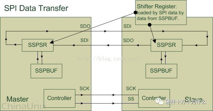 SSPSR is the internal shift register of the SPI device. Its main function is to move data in and out of SSPBUF based on the state of the SPI clock signal, with the data size determined by Bus-Width and Channel-Width.
Bus-Width specifies the unit of data transfer between the address bus and the master device.
For example, if we want to write 16 Bytes of data to the SSPBUF of the master device, we first set the Bus-Width of the master device’s configuration register to Byte; then we write data to the master device’s Tx-Data shift register at the address bus entry, writing 1 Byte at a time (using the writeb function); after writing 1 Byte, the Tx-Data shift register of the master device will automatically move the 1 Byte of data from the address bus into SSPBUF; this action needs to be repeated 16 times.
Channel-Width specifies the unit of data transfer between the master and slave devices. Similar to Bus-Width, the internal shift register of the master device will automatically move data from Master-SSPBUF to Slave-SDI through the Master-SDO pin, and Slave-SSPSR will move each received data into Slave-SSPBUF. Typically, Bus-Width is always greater than or equal to Channel-Width to ensure that the data exchange frequency between the master and slave does not exceed the data exchange frequency between the address bus and the master, preventing invalid data from being stored in SSPBUF.
3.4 SSPBUF
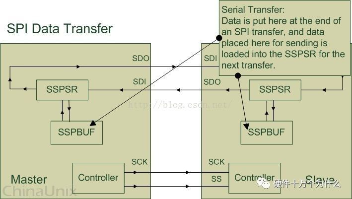
We know that during each clock cycle, the data exchanged between the master and slave is actually copied from the SPI’s internal shift register to SSPBUF. We can control the SPI device’s internal SSPBUF indirectly by reading and writing data to the corresponding registers (Tx-Data / Rx-Data register) of SSPBUF.
For example, before sending data, we should first write the data to be sent into the Tx-Data register of the master. This data will be automatically moved into the Master-SSPBUF by the Master-SSPSR shift register according to the Bus-Width, and then the data will be moved out from Master-SSPBUF according to the Channel-Width through the Master-SDO pin to the Slave-SDI pin. The Slave-SSPSR will then move the received data from Slave-SDI into Slave-SSPBUF. Meanwhile, the data in the Slave-SSPBUF will be sent to Master-SDI through Slave-SDO based on the size of the received data (Channel-Width), and the Master-SSPSR will move the received data from Master-SDI into Master-SSPBUF. After a single data transmission is complete, the user program can read the data obtained from the Master device’s Rx-Data register.
3.5 Controller
The controller inside the master device primarily controls the slave device through the clock signal and slave select signal. The slave device will wait until it receives the slave select signal from the master, and then operate according to the clock signal.
The master device’s slave select operation must be implemented by the program. For example, the program pulls down the clock signal on the SS/CS pin to initiate the data communication with the SPI device; when the program wants to end data communication, it raises the clock signal on the SS/CS pin.
4. Example of SPI
Having discussed so much, I will now provide an example to help everyone understand.
SPI is a ring bus structure composed of SS (CS), SCK, SDI, and SDO, and its timing is quite simple, mainly under the control of SCK, where two bidirectional shift registers exchange data.
Assuming the following 8-bit register holds the data to be sent 10101010, data is sent on the rising edge and received on the falling edge, with the high bit sent first.
Then, on the first rising edge, the data will be SDO=1; the register will be 0101010x. When the falling edge comes, the level on SDI will be stored in the register, so now the register will be 0101010SDI. After 8 clock pulses, the contents of the two registers will have exchanged once. This completes one SPI timing.
For example, suppose the master and slave are initialized and ready, with the master’s sbuff=0xaa and the slave’s sbuff=0x55. Below, I will demonstrate the data situation of SPI over 8 clock cycles step by step: assuming data is sent on the rising edge.
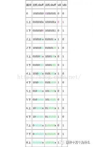
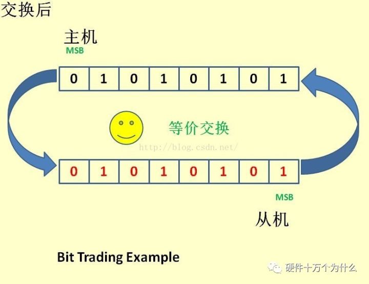
This completes the exchange of 8 bits between the two registers. The above indicates the rising edge, and the below indicates the falling edge, with SDI and SDO relative to the master. This understanding is quite close; the next step is to transform the above process into an animation.

End
“Automotive Electronics Embedded” is synchronously launched on CSDN, focusing on the path of AUTOSAR improvement, where each module is introduced in detail according to the actual project development and maintenance process.Core concepts, actual requirements, engineering configurations, special requirements, and practical experience summaries are provided.The goal is to enable readers to understand the principles and complete module configurations or solve problems based on needs after reading each chapter.”
Click the last part of the article“Read the Original” in the lower left cornerto get more information.
Orcopy the link below to your browserto get more information.
https://blog.csdn.net/qq_36056498/article/details/132125693
Note: This article uses some third-party tools and documents. If there are any infringements, please contact the author for deletion!
Recommended Reading
Summary of Exciting Articles in Automotive Electronics Embedded, Issue 1: 20210530-20230703
Detailed Explanation of EcuM Wake-up Source Events under AUTOSAR Architecture
Analysis of Continuous Write and Default Value Issues in NVM Block under AUTOSAR Architecture
Detailed Analysis of NvM Module under AUTOSAR Architecture
Analysis of Message Drop Timeout Issue under AUTOSAR Architecture
Overview of Ethernet Communication Architecture under Classic Autosar
Service-Oriented Communication with Someip Middleware
Detailed Analysis of Fee under AUTOSAR Architecture
Introduction to FLASH Basic Concepts of TC37x Chip
Detailed Analysis of Fls under AUTOSAR Architecture
Introduction to DMU of TC3xx Chip
Introduction to MPU of TC3xx Chip
Detailed Explanation of Trap in TC3xx Chip
End
Thank you for your likes, follows, shares, and views. Your encouragement is my greatest motivation!
Automotive Electronics Embedded
Scan the QR code to follow my public account