1. Introduction to SPI
SPI, short for Serial Peripheral Interface, is a serial communication interface defined by Motorola for its MC68HCXX series processors. The SPI interface is mainly used between EEPROM, FLASH, real-time clocks, AD converters, as well as digital signal processors and digital signal decoders. SPI is a high-speed, full-duplex, synchronous communication bus that only occupies four pins on the chip, saving pin space and providing convenience for PCB layout. Due to this simple and easy-to-use feature, more and more chips are integrating this communication protocol.
2. Features of SPI
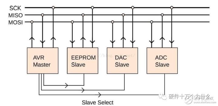
2.1 Master-Slave Control Mode
SPI specifies that communication between two SPI devices must be controlled by a master device. A master device can control multiple slave devices by providing a clock and selecting the slave device through Slave Select (SS). The SPI protocol also stipulates that the clock for the slave device is provided by the master device through the SCK pin; the slave device cannot generate or control the clock. Without a clock, the slave device cannot function properly.
2.2 Synchronous Data Transmission
The master device generates corresponding clock pulses based on the data to be exchanged. These clock pulses form the clock signal, which controls when data is exchanged and when received data is sampled between the two SPI devices, ensuring that data is transmitted synchronously.
2.3 Data Exchanges
The data transfer between SPI devices is referred to as data exchange because the SPI protocol specifies that an SPI device cannot act solely as a “transmitter” or “receiver” during data communication. In each clock cycle, SPI devices send and receive one bit of data, meaning that one bit of data is exchanged. A slave device must be accessed by the master device to receive control signals sent from the master. Therefore, the master must first select the slave device through the SS/CS pin. During data transmission, each received data must be sampled before the next data transmission. If the previously received data is not read, it may be discarded, causing the SPI physical module to fail. Hence, in programs, it is common to read the data from the SPI device after the SPI transmission is complete, even if this data (dummy data) is useless in our program.
2.4 Four Transmission Modes of SPI
There are four transmission modes: rising edge, falling edge, leading edge, and trailing edge. There are also MSB and LSB transmission methods.
2.5 Only Master and Slave Modes
There is no concept of read and write, as each SPI operation involves data exchange between master and slave devices. This means that sending data will always result in receiving data; to receive data, one must also send data first.
3. Working Mechanism
3.1 Overview
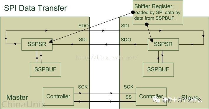
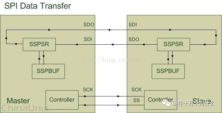 The above diagram is a simple description of communication between SPI devices. Below, we will explain the components shown in the diagram: SSPBUF, Synchronous Serial Port Buffer, which refers to the internal buffer of the SPI device, usually in FIFO form, storing temporary data during transmission; SSPSR, Synchronous Serial Port Register, which refers to the shift register in the SPI device, responsible for shifting data in or out of SSPBUF according to the set bit width; Controller, which refers to the control register within the SPI device, which can be configured to set the transmission mode of the SPI bus. Typically, we only need to program the four pins described in the diagram to control data communication between the SPI devices: SCK, Serial Clock, primarily used for the master device to transmit clock signals to the slave device, controlling the timing and rate of data exchange; SS/CS, Slave Select/Chip Select, used for the master device to select the slave device, allowing the selected slave device to be accessed by the master; SDO/MOSI, Serial Data Output/Master Out Slave In, also referred to as Tx-Channel on the master, serves as the data output for sending data from the SPI device; SDI/MISO, Serial Data Input/Master In Slave Out, also referred to as Rx-Channel on the master, serves as the data input for receiving data from the SPI device; During communication, a data loop is created between the master and slave devices, as illustrated in the diagram, with data being shifted in and out of SSPBUF controlled by SSPSR and the communication mode determined by the controller, while SCK transmits the clock signal.
3.2 Timing
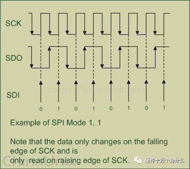 The above diagram illustrates the working mechanism of the SPI protocol by exchanging 1 Byte of data between the master and slave devices. First, let’s explain the concepts of phase and polarity.
3.2.1 Abbreviations or Terms Related to SPI
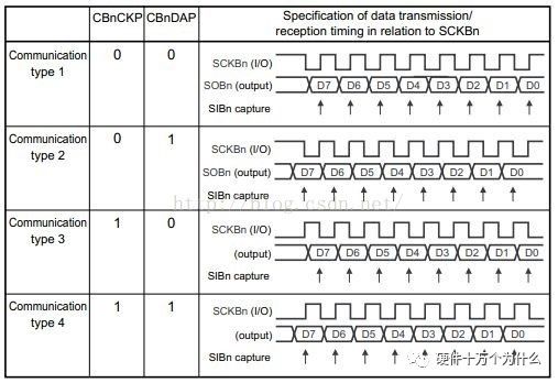
The polarity and phase of SPI, commonly written as CPOL and CPHA, can also be referred to by other terms. A brief summary is as follows: (1) CKPOL (Clock Polarity) = CPOL = POL = Polarity; (2) CKPHA (Clock Phase) = CPHA = PHA = Phase; (3) SCK=SCLK=SPI clock; (4) Edge refers to the moment when the clock level changes, either rising edge or falling edge. Within a clock cycle, there are two edges, referred to as: Leading edge = first edge; Trailing edge = second edge.
3.2.2 Phase and Polarity of SPI
CPOL and CPHA can each be 0 or 1, leading to four combinations: Mode 0 CPOL=0, CPHA=0; Mode 1 CPOL=0, CPHA=1; Mode 2 CPOL=1, CPHA=0; Mode 3 CPOL=1, CPHA=1.
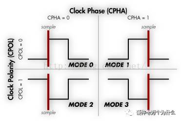
3.2.3 CPOL Polarity
CPOL indicates the idle state of SCLK, which is the state before and after sending 8 bits of data. When SCLK is idle, its level can be either low (0) or high (1): CPOL=0 indicates that the idle level is low, thus when SCLK is active, it is high (active-high); CPOL=1 indicates that the idle level is high, thus when SCLK is active, it is low (active-low).
3.2.4 CPHA Phase
Capture strobe, latch, read, and sample all refer to data sampling, which indicates the moment data is valid. The phase corresponds to which edge the data is sampled on, either the first or second edge. 0 corresponds to the first edge, while 1 corresponds to the second edge.
3.2.5 How to Set SPI Polarity and Phase in Software
SPI consists of master and slave devices that communicate via the SPI protocol. The mode of the slave device determines the master device’s mode. Therefore, one must first understand the slave device’s SPI mode and then configure the master device’s SPI mode to match the slave’s mode for proper communication.
3.2.5.1 Fixed Mode Determined by Slave Device Hardware
The specific mode of the SPI slave device is described in the datasheet, which must be consulted to find out whether the idle state is high or low, determining CPOL. Then, based on whether the device samples data on the rising or falling edge, one can deduce CPHA.
3.2.5.2 Configurable Mode Set by Software
The slave device is also an SPI controller that supports all four modes; thus, it can be set to any mode. After determining the slave device’s mode, the master device’s mode should be configured to match the slave’s mode for communication.
3.3 SSPSR
 SSPSR is the internal shift register of the SPI device. Its main function is to shift data in or out of SSPBUF based on the state of the SPI clock signal, with the amount of data shifted determined by Bus-Width and Channel-Width.
3.4 SSPBUF
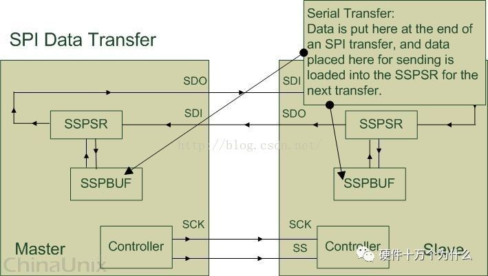 During each clock cycle, the data exchanged between the master and slave is actually copied from the SPI’s internal shift register to SSPBUF. We can indirectly control the SPI device’s internal SSPBUF by reading and writing data to the corresponding Tx-Data/Rx-Data registers. For example, before sending data, we should write the data to be sent to the master’s Tx-Data register, which will automatically be shifted into Master-SSPBUF by the Master-SSPSR based on Bus-Width. Then this data will be shifted out from Master-SSPBUF via Master-SDO to the Slave-SDI, while Slave-SSPSR shifts the received data into Slave-SSPBUF. Simultaneously, the data in Slave-SSPBUF is sent to Master-SDI through Slave-SDO, and Master-SSPSR shifts the received data into Master-SSPBUF. After the data transfer is complete, the user program can read the exchanged data from the Master device’s Rx-Data register.
3.5 Controller
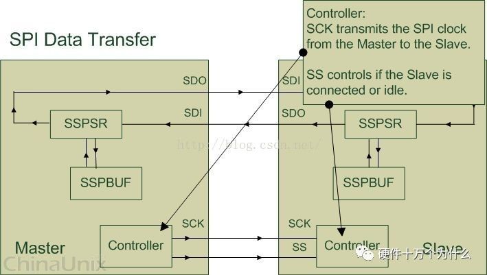 The Controller in the master device primarily controls the slave device through clock signals and slave select signals. The slave device waits until it receives the slave select signal from the master, after which it operates based on the clock signal. The master’s selection operation must be implemented in software. For instance, the program pulls the SS/CS pin low to initiate SPI data communication; when the program wants to end communication, it pulls the SS/CS pin high.
4. Example of SPI
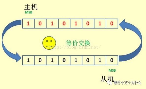
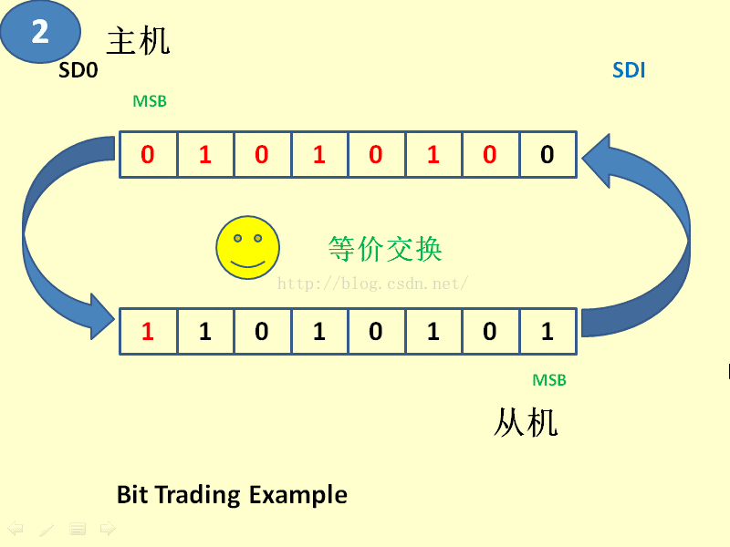
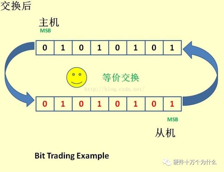
Having discussed so much, let me provide an example to help everyone understand. SPI is a ring bus structure consisting of SS (CS), SCK, SDI, and SDO, where the timing is quite simple, primarily under the control of SCK, with two bidirectional shift registers exchanging data. Assume the 8-bit register contains the data 10101010, sending on the rising edge and receiving on the falling edge, with high bits sent first. When the first rising edge occurs, the data will be SDO=1; the register will then be 0101010x. When the falling edge arrives, the level on SDI will be stored in the register, resulting in the register being 0101010sdi. Thus, after 8 clock pulses, the contents of the two registers will have exchanged once. This completes one SPI timing sequence. For example, suppose the master and slave are initialized and ready, and the master’s sbuff=0xaa while the slave’s sbuff=0x55; below, I will demonstrate the data situation for the 8 clock cycles of SPI step by step: assuming data is sent on the rising edge.
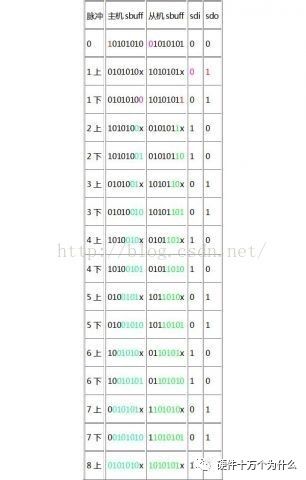 This completes the 8-bit exchange between the two registers, with the upper part indicating the rising edge and the lower part indicating the falling edge, SDI and SDO relative to the master. This is very close to understanding; the next step is to animate the above process.

This article is reprinted from CSDN, and in the future, we will release a video tutorial on the debugging process of the LoRa module’s SPI interface. Stay tuned.
Join the group for discussions; to join, add the WeChat friend hw100k, mentioning “SPI” or “LoRa” to request group entry.