1. Industry Trends: Semiconductor Cycle Inflection Point, Domestic Substitution Emerging
1.1 Semiconductor Industry: A Major Cycle of About Ten Years, Demand Driven by Technological Development
The global semiconductor industry market size reached $580.1 billion in 2022, hitting a historical high, with a compound annual growth rate of 7.4% over the past decade. By analyzing the year-on-year growth rate of global semiconductor sales over the past 20 years, it is found that the semiconductor industry has a major cycle of about 10 years, characterized by an “M” shaped fluctuation every ten years. This is mainly due to changes in global GDP growth rates and technological advancements driving industry development. In the first half of 2023, the global semiconductor industry is in a downward cycle, but the new round of technological innovation brought by AIGC has significantly increased demand, and the industry is expected to enter an upward cycle in 2024.
Figure: Global Semiconductor Shows Volatile Growth, Major Cycle Every Ten Years
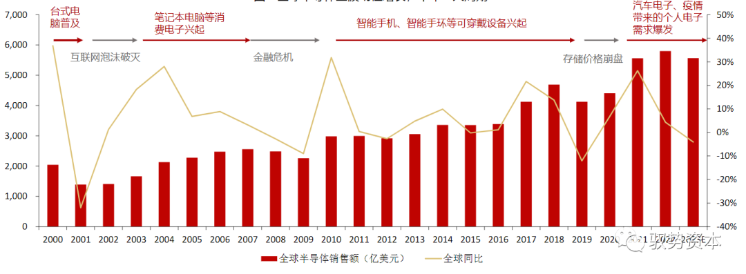
Source: Encyclopedia of Integrated Circuit Industry, WSTS, iFinD, Zhejiang Securities Research Institute
The major cycle is driven by technology, while the minor cycle is influenced by downstream demand cycle fluctuations. From the perspective of year-on-year global semiconductor sales, the industry minor cycle is about 3 years. The last peak of the cycle was in August 2021. In January 2023, global semiconductor sales were $41.3 billion, a year-on-year decrease of 19%. Based on industry cycle judgment, it is expected that the second half of 2023 will welcome the inflection point of the downward cycle. In 2024, on one hand, traditional chips will reach inventory inflection points, and on the other hand, the significant increase in computing power demand driven by AIGC will lead to an explosion in demand for emerging chips, accelerating the arrival of the upward cycle.
Figure: Global Semiconductor Minor Cycle is About 3 Years
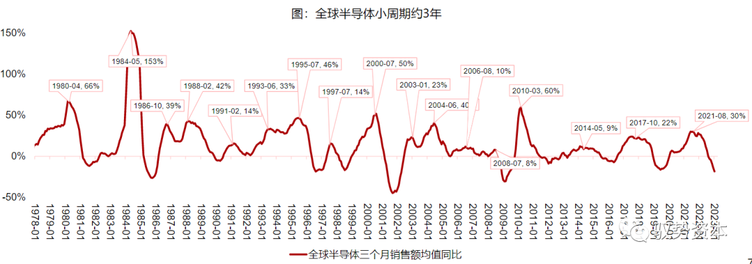
Source: Semiconductor Industry Association of America, Zhejiang Securities Research Institute
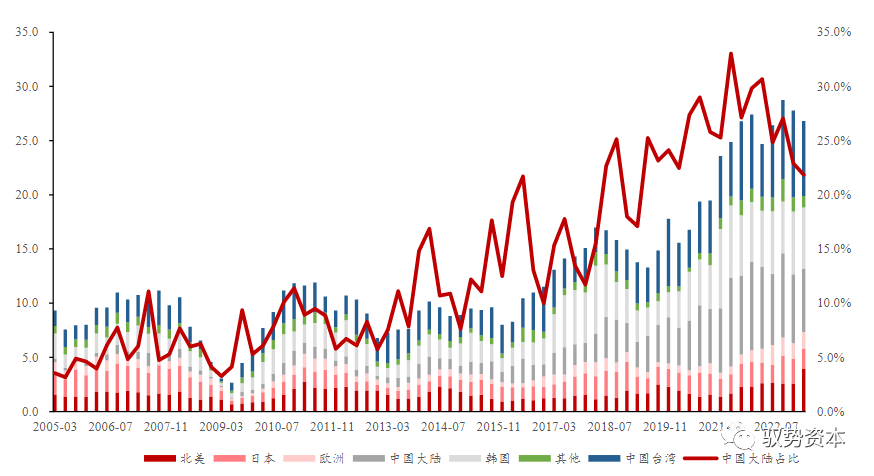
From 2012 to 2022, the global and Chinese semiconductor equipment market sizes had compound annual growth rates of 11% and 27%, respectively, with China’s growth rate outpacing the global average. Mainland China is the largest semiconductor equipment market globally. In 2022, the global semiconductor equipment market was $107.6 billion, with semiconductor equipment sales in mainland China accounting for 26% of global sales, reaching $28.3 billion, surpassing Taiwan (25%), South Korea (20%), and North America (10%), making it the largest semiconductor equipment market for three consecutive years.
Figure: China’s Share in the Global Equipment Market Increased from 6% in 2006 to 26% in 2022
Source: SEMI, Japan Semiconductor Equipment Association, Zhejiang Securities Research Institute
1.2 Semiconductor Equipment: Shrinking Chip Processes Drive Increased Capital Expenditure on Equipment
As chip processes shrink, capital expenditure on equipment increases, driving growth in the semiconductor equipment market. Historically, chip development has always followed Moore’s Law. The core of Moore’s Law is that the number of transistors that can be accommodated on an integrated circuit doubles approximately every 18 to 24 months. The essence of Moore’s Law is an economic law. As chip processes continue to shrink, Moore’s Law is gradually losing its effectiveness. In 2018, the gap between actual chip performance and the demands of Moore’s Law expanded by 15 times. With the failure of Moore’s Law, the shrinking chip processes have led to a rapid increase in construction costs, driving up capital expenditures on equipment. The construction cost for a fab producing 10,000 5nm chips is as high as $5.4 billion, which is six times that of 28nm.
Figure: Construction Costs for 10,000 Wafer Fab (in $100 million)
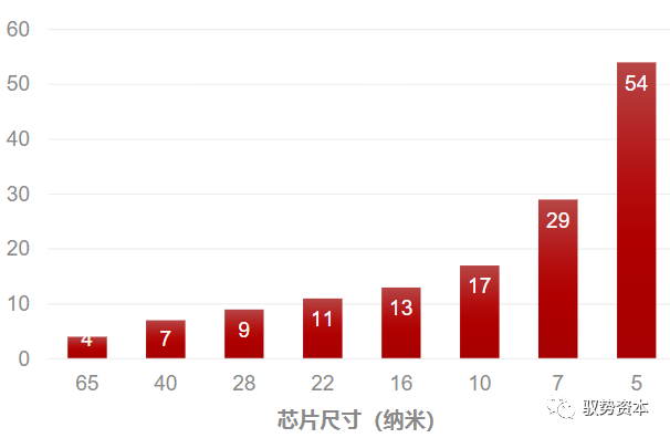
Figure: Leading Logic Chip Manufacturers’ Process Development Roadmap
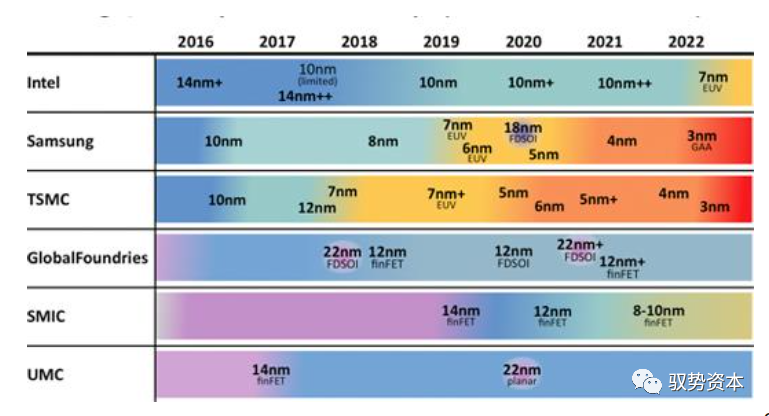
Source: IBS, McKinsey, IC Insights, Zhejiang Securities Research Institute
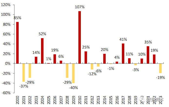
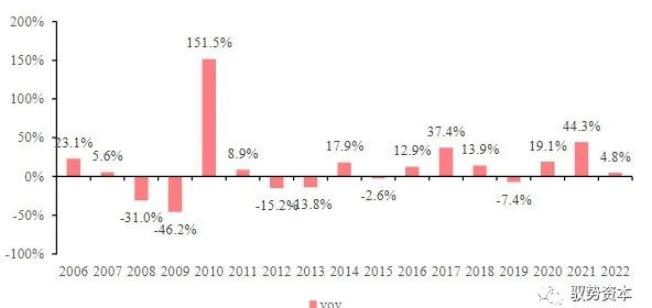
Global semiconductor capital expenditure: IC Insights expects global semiconductor capital expenditure to reach $181.7 billion in 2022, a year-on-year increase of 19%. Due to a weak memory market and U.S. sanctions against China, global semiconductor equipment capital expenditure is expected to be $146.6 billion in 2023, a year-on-year decrease of 19%.
From a cyclical analysis perspective: looking at the year-on-year growth rate of global semiconductor capital expenditure from 2000 to the present, global semiconductor capital expenditure has a cycle of about 3 years. The year 2023 is at the bottom of the industry cycle, and it is expected that capital expenditure will reverse in 2024.
Figure: Global Semiconductor Industry Capital Expenditure
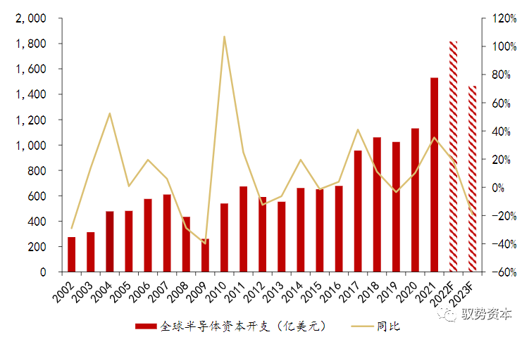
Figure: Global Semiconductor Capital Expenditure Cycles, About 3 Years Per Cycle
Source: IC Insights, McKinsey, Zhejiang Securities Research Institute
1.3 Semiconductor Equipment: U.S.-Japan-Netherlands Semiconductor Equipment Blockade Forces Rapid Increase in Domestic Substitution Rate
Since 2018, the U.S. has continuously intensified semiconductor controls against China, extending from downstream companies like Huawei, ZTE, and SMIC to upstream companies. On October 7, 2022, the U.S. BIS expanded semiconductor controls against China to include advanced chips, equipment, components, and personnel. The scope of U.S. semiconductor equipment controls includes advanced logic process chips below 16/14nm, NAND flash memory chips with more than 128 layers, and DRAM memory chips with a half-pitch of 18nm or lower.
Figure: Continuous Expansion of U.S. Semiconductor Sanctions Against China, Advanced Equipment Included in Export Ban
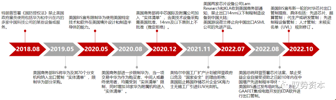
Source: Chip Research, Zhejiang Securities Research Institute
The trend of de-globalization in the semiconductor industry has emerged, with countries actively formulating supportive policies to promote the development of local semiconductor industries since 2022. On March 10, 2023, the decision of the First Session of the 14th National People’s Congress restructured the Ministry of Science and Technology and established a Central Science and Technology Committee, which is conducive to coordinating various forces for technological innovation, promoting the improvement of a new national system, optimizing the management of the entire chain of technological innovation, and promoting the transformation of scientific and technological achievements, as well as the integration of technology with economic and social development. On April 6, 2023, the National Integrated Circuit Standardization Technical Committee was established, which plays an important role in promoting the high-quality development of the integrated circuit industry.
Figure: Global Semiconductor Industry Policies of Various Countries in 2022
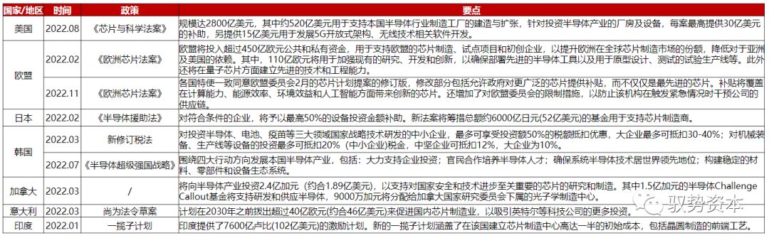
Source: Jiwei Network, Zhejiang Securities Research Institute
2. Process Control: Measurement and Inspection are Important Guarantees for Semiconductor Manufacturing Yield
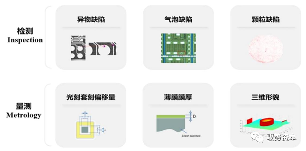
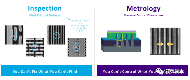
Process control: In the semiconductor wafer manufacturing process, various processes often require size measurement, defect detection, etc., for process control and yield management, requiring speed and accuracy. Size measurement, defect detection, etc., are applied after each process. IC measurement equipment is used for process control and yield management, with detection requirements for speed, accuracy, and non-destructive testing. In the development of IC measurement, there are various technical difficulties in size miniaturization, complex 3D structures, and new materials, facing various upgrading demands from different semiconductor detection needs such as memory, CIS, and compound semiconductors. The technical categories of IC measurement equipment include probe microscopes, scanning/transmission electron microscopes, optical microscopes, ellipsometers/scatterometers, etc. The direction of technological development includes continuing existing non-destructive measurement technologies, advancing parallel electron beam technology in electron microscopy, extending scatterometry to EUV and X-ray to reduce wavelengths, and integrating multiple measurement methods with machine learning to achieve hybrid measurement.
Process control equipment includes measurement equipment (Metrology) and defect (including particle) inspection equipment used in the process. In the chip production process, online process inspection equipment must perform non-destructive quantitative measurements and inspections on wafers after various processes to ensure that the critical physical parameters of the process (such as film thickness, line width, trench/hole depth, side wall angle, etc.) meet the requirements, while identifying potential defects and classifying them to eliminate non-compliant wafers, avoiding waste in subsequent processes. Another role of process inspection equipment is to assist in optimizing equipment operating parameters and photomask design during process development and pilot production, optimizing the entire process flow, shortening development time, improving yield, and achieving mass production.
Semiconductor Measurement Metrology Mainly Includes:
1) Measurement of alignment deviation in overlay; 2) Measurement of film material thickness; 3) Measurement of critical dimensions (CD) after wafer exposure and development, etching, and CMP processes; 4) Others: such as wafer thickness, bow/warp, 1D/2D stress, wafer morphology, four-point probe measurement of resistance (RS), XPS measurement of doping content, etc., AFM (Atomic Force Microscope)/Metal plus (ultrasonic) measurement of step height, etc.
Semiconductor Inspection Mainly Includes:
1) Non-pattern defect detection, including particles, residues, scratches, and native pits (COP); 2) Pattern defect detection, including breaks, line edge defects, bridging, deformation, etc.; 3) Mask defects detection, including particles, etc.; 4) Defect re-inspection, confirming the existence of detected defects (location, size, type) using optical microscopes or scanning electron microscopes.
Figure: Classification of Semiconductor Measurement and Inspection
Source: Zhongke Feicai Prospectus, Founder Securities Research Institute
Middleway Testing focuses on advanced packaging processes, mainly for chip flip-chip, wafer-level packaging (WLP), and through-silicon vias (TSV), requiring non-contact quantitative inspection and measurement of bumps, vias, copper pillars, and their consistency in shape, spacing, and height, as well as the redistribution layer (RDL). Backend testing mainly utilizes electrical testing for chip functionality and electrical parameter testing, primarily including wafer testing and finished product testing.
Figure: Market Space for Process Control (Detection, Measurement) and ATE (Testing) in 2021
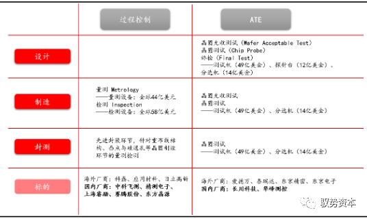
Source: Gartner, Huajing Industry Research Institute, Founder Securities Research Institute
Figure: Detecting Defects & Measuring Dimensions
Source: KLA, Founder Securities Research Institute
Depending on the different materials and structures used in the manufacturing process, process inspection equipment employs various technologies including wide-band optical (UV to infrared), electron beam, laser, and X-ray. In terms of performance indicators, as processes continue to advance towards finer line widths, the device morphology structure is also transitioning from two-dimensional planar structures to three-dimensional structures. Thus, higher requirements are imposed on the sensitivity, applicability, stability, and throughput of detection equipment.
Figure: Comparison of Optical Detection Technology, Electron Beam Detection Technology, and X-ray Measurement Technology Features
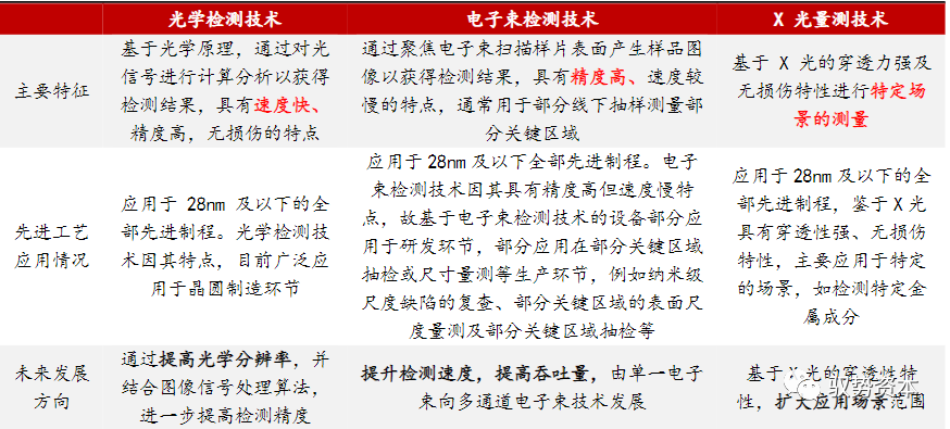
Source: Zhongke Feicai Prospectus, Founder Securities Research Institute
Devices using optical detection technology can relatively well achieve a balance of high precision and high speed, and can meet functions that other technologies cannot achieve, such as three-dimensional morphology measurement, lithography overlay measurement, and multilayer film thickness measurement. Therefore, this method is predominant. According to VLSI Research and QY Research, in 2020, the market shares of optical detection technology, electron beam detection technology, and X-ray measurement technology in the global semiconductor detection and measurement equipment market were 75.2%, 18.7%, and 2.2%, respectively.
Figure: Process Control Classification and Market Size in 2021 (in $100 million)
Source: Gartner, Founder Securities Research Institute
2.1 Measurement
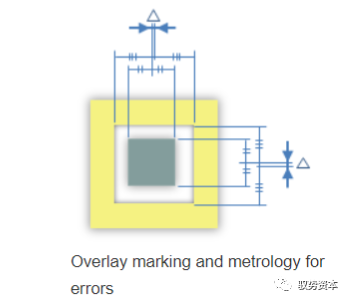
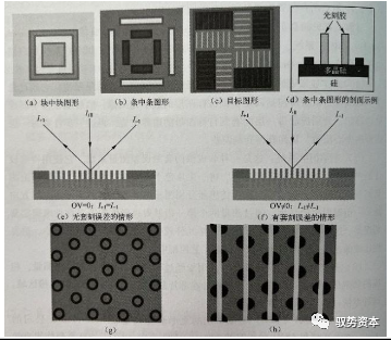
Overlay accuracy measurement equipment: Used to measure the overlay error between layers, which is the planar distance between the centers of two layer patterns. There are three main measurement systems: optical microscope imaging (IBO) system, optical diffraction (DBO) system, and scanning electron microscope (SEM-OL) system. The optical microscope imaging system is the most commonly used, calculating overlay errors through imaging; the optical diffraction system uses a non-imaging method, measuring the intensity of the diffracted beam with a light intensity sensor to determine overlay errors, using fewer optical elements, and is commonly used in advanced lithography process control; the scanning electron microscope system is mainly used for final overlay error measurement after etching, with slower measurement speeds.
The target patterns for overlay accuracy measurement are typically made in the scribing groove area, and the target patterns for imaging overlay measurement systems usually include (a) block in block, (b) line in line, and (c) aim (AIM) patterns.
Figure: Overlay Error Measurement

Figure: Common Target Patterns for Overlay Error Measurement
Source: Hitachi High-Tech Official Website, Founder Securities Research Institute, “Encyclopedia of Integrated Circuit Industry”, Qihong Semiconductor
Common optical overlay equipment includes KLA’s Archer series and ASML’s YieldStar series. The Archer series uses IBO and DBO measurement technologies to measure various overlay target patterns; YieldStar uses DBO measurement technology; Hitachi’s CD-SEM CV series uses high-voltage accelerated scanning electron microscope (SEM-OL).
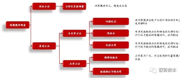
Film thickness measurement: After multiple deposits of various materials on the wafer, it is necessary to accurately judge the film thickness and other parameter properties to ensure that the product meets performance design requirements. There are many methods to measure film thickness; traditional methods mainly involve direct measurement using a step profiler, but this method can be quite destructive to the film itself, and the measurement results are greatly influenced by instrument accuracy, making precise measurements costly. Currently, the most commonly used methods mainly include non-optical and optical methods. Non-optical methods can only be used for measuring film thickness, mainly including four-probe method, eddy current method, capacitive method, electromagnetic methods, etc., with the four-probe and eddy current methods being more widely applied; optical methods for measuring film thickness mainly include prism coupling guided mode method, optical cutting method, multi-beam interference method, spectrophotometric measurement method, ellipsometry, etc. Among these, the ellipsometry method is the most widely used and can simultaneously measure the optical parameters of the film.
Figure: Film Measurement Methods
Source: “Film Thickness Measurement Based on Ellipsometry”, Founder Securities Research Institute
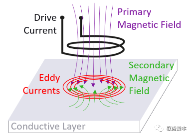
The four-probe method (4PP) refers to using four equidistant metallic probes to contact the surface of the film material. The outer two probes pass direct current, while the two middle probes connect to a voltmeter to measure the voltage drop. Based on the measured voltage and current, the resistance at a specific location is obtained, and the film thickness is calculated by dividing the resistivity of the film material by the obtained resistance, generally calculated through software. The eddy current method (EC) refers to generating time-varying eddy currents in the conductive layer through a time-varying current in a coil. These time-varying eddy currents generate a magnetic field that alters the impedance of the driving coil, which is inversely proportional to the resistance of the film material, allowing for the calculation of film thickness parameters.
Figure: Four-Probe Method
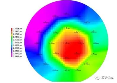
Figure: Eddy Current Method
Source: KLA, Founder Securities Research Institute Data
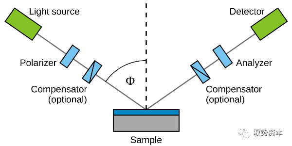
The basic principle of the ellipsometry method is to illuminate a sample with a beam of elliptical polarized light at a certain angle of incidence. Given the polarization state of the incident light, the specific structure of the film material can be determined based on the change in polarization state, obtaining its thickness and optical parameter information (such as complex refractive index, thickness, or complex dielectric constant).
Figure: Ellipsometry Principle Diagram
Source: Wikimedia, Founder Securities Research Institute
Currently, the main products for non-optical measurement of film thickness are KLA’s Filmetrics R50 series, while the main products for optical measurement of film thickness include KLA’s Aleris series and SpectraFilm series. Domestic optical measurement film thickness products include Shanghai Jingce’s EFILM series.
Chart 14: Filmetrics R50, Aleris, and SpectraFilm in Order
Source: KLA, Founder Securities Research Institute
Critical dimension measurement equipment: Mainly used for online measurement of critical dimensions (CD), height, and side wall angles during the chip production process, as well as performance monitoring of critical equipment (lithography machines, coating and developing equipment, etc.). Critical dimension measurement is mainly used for after-development inspection (ADI) and after-etch inspection (AEI). Currently, it mainly relies on the non-imaging measurement technology of optical scatterometers, which are also called optical critical dimension measurement instruments (OCD). Their principle is to reconstruct the three-dimensional morphology of the sample by measuring the scattering information of the sample and solving the inverse scattering problem.
Figure: Basic Process of Optical Scatter Measurement
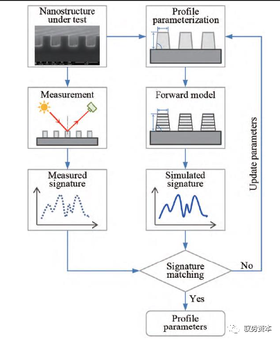
Source: “Online Optical Measurement and Detection Technology in Integrated Circuit Manufacturing: Status, Challenges, and Trends”, Founder Securities Research Institute
The basic process of OCD measurement mainly includes two important steps: the forward problem and the inverse problem. The forward problem involves obtaining the scattering information of the sample structure through a certain scattering measurement device, which requires solving the instrument measurement problem. The inverse problem requires extracting the three-dimensional morphology parameters of the sample from the measured scattering data, which requires constructing a forward scattering model of the interaction between light and the sample structure and selecting an appropriate solving algorithm.
Measurement instruments: Currently, the main optical scattering devices used can be divided into angle-resolved scatterometers and spectral scatterometers. The advantage of angle-resolved scatterometers lies in that they use a single wavelength, eliminating the need to hypothesize the dielectric function of the sample material during data analysis; additionally, they can relatively easily extend to shorter wavelength ranges, such as EUV and X-ray. Their disadvantage is that they contain moving components, which limit measurement speed. The advantage of spectral scatterometers is their very fast measurement speed; a commonly used type is based on spectral ellipsometry (SE) scatterometers, which can achieve very high vertical resolution, obtaining more measurement information compared to angle-resolved scatterometers. Their disadvantage is that precise calibration is needed for accurate measurement, especially in ellipsometric scattering measurements, and the optical constants of the sample material need to be predetermined over a wide spectral range. In practice, to improve measurement sensitivity, both scattering measurement methods are usually combined.
Figure: Schematic Diagram of Different Optical Scattering Measurement Devices Note: (a)(b) Angle-Resolved Scatterometers; (c)(d) Spectral Scatterometers
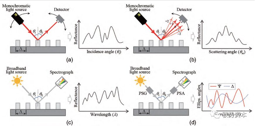
Source: “Online Optical Measurement and Detection Technology in Integrated Circuit Manufacturing: Status, Challenges, and Trends”, Founder Securities Research Institute
Constructing a forward scattering model and selecting a solving algorithm: In optical scattering measurement, extracting the three-dimensional morphology parameters of the sample from scattering measurement data is essentially the process of solving the inverse scattering problem. Currently, there are two main solving methods: library matching method and nonlinear regression method. In the parameter extraction process of library matching, a scattering simulation database is established in advance, and the measured data is compared with the simulation data to obtain the best match between the measured data and the corresponding sample parameter value. The advantage of the library matching method is that it can quickly extract the parameters to be measured, but it requires the prior establishment and storage of a large simulation database, and the accuracy is limited by the grid spacing of the database. The advantage of the nonlinear regression method is that it does not require the establishment of a simulation database and can yield relatively accurate results, but it is very time-consuming because it requires calling the forward scattering model to compute simulation data for each iteration.
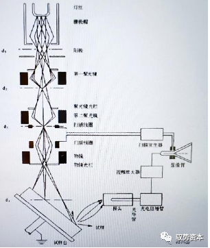
In addition to OCD, Atomic Force Microscopes (AFM) and Scanning Electron Microscopes (SEM) are also the two most widely used instruments for measuring micro-nano line spacing dimensions. The lateral resolution of the images obtained by both is similar. AFM provides a three-dimensional image of the surface morphology of the measured product, while SEM can only provide a two-dimensional image but has a large depth of field and a wide field of view. Critical Dimension Scanning Electron Microscope (CD-SEM) is a type of scanning electron microscope that can automatically locate and measure line widths, widely used for monitoring line widths in semiconductor production lines.
The scanning electron microscope works by exploiting the differences in surface features of the material; under the action of the electron beam, different brightness differences are produced in different areas of the sample, thus obtaining images with a certain contrast. The imaging signals are secondary electrons, backscattered electrons, or absorbed electrons, with secondary electrons being the primary imaging signal. High-energy electron beams bombard the surface of the sample, exciting various physical signals from the surface of the sample, which are then detected by different signal detectors to convert the physical signals into image information.
Figure: Interaction of Electron Beams with Matter Producing Information
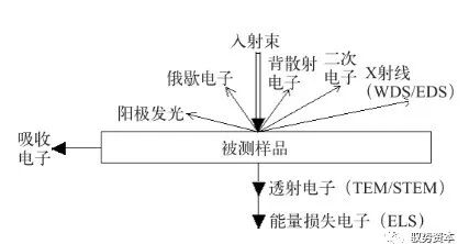
Figure: Schematic Diagram of Scanning Electron Microscope Principle
Source: “Application Examples of SEM in Semiconductor Process Research”, Founder Securities Research Institute Data Source: Shuosibai Testing, Founder Securities Research Institute
Algorithm: After obtaining the measurement images of the patterns, CD-SEM performs measurements and uploads the data. The measurement algorithms of CD-SEM need continuous optimization and improvement to ensure that the measurement results accurately reflect the performance of the samples. For example, new measurement methods have been introduced, including edge roughness, gap, wiggling, overlay, center gravity, etc. Additionally, there is a continuous need to improve measurement reliability and sensitivity to fluctuations in product processes.
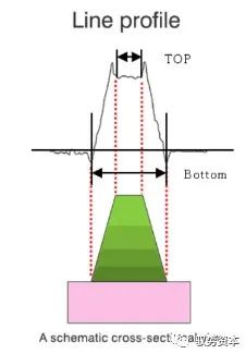
Figure: SEM Images
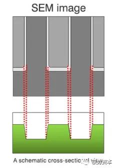
Figure: Creating a Line Profile from SEM Images to Calculate Measured Values
Source: Hitachi High-Tech Official Website, Founder Securities Research Institute
2.2 Detection
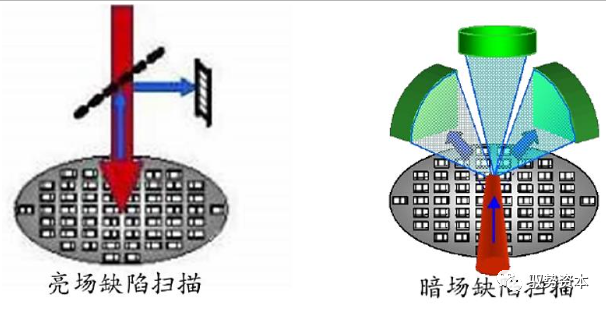
Pattern wafer defect detection: Optical pattern wafer defect detection equipment detects and identifies defects and contamination on wafers using high-precision optical detection technology, providing wafer fabs with product quality issues at different production nodes and confirming whether the operation of process equipment is normal, thereby improving yield and saving costs. Optical detection technology captures images of circuit patterns on wafer surfaces using wide-spectrum illumination from deep UV to visible light or high-power laser illumination at a single wavelength in deep UV, employing high-resolution bright field or dark field imaging methods to perform real-time alignment, noise reduction, analysis of circuit patterns, and identification and classification of defects.
Optical pattern wafer defect detection equipment is divided into bright field and dark field categories. The main difference between the two is that bright field equipment analyzes defects by collecting vertically reflected light signals from the wafer surface, while dark field equipment analyzes defects by collecting scattered light signals from the wafer surface. If the wafer surface is smooth and defect-free, the light reflected back by bright field equipment is relatively complete incident light, whereas the incident light of dark field equipment is fully reflected, receiving scattered light signals.
As the equipment industry continues to develop, the definitions of bright field and dark field are also changing. Currently, bright field generally refers to the illumination and collection optical paths sharing the same microscope objective near the wafer, while dark field refers to the illumination and collection optical paths being completely separated in physical space. Due to the differences in vertical reflection and scattered light signals, the detection sensitivity of bright field equipment is higher than that of dark field equipment, but bright field equipment also has a slower scanning speed.
Chart 23: Bright Field and Dark Field Optical Pattern Wafer Defect Detection Equipment
Source: “Detection and Yield Improvement of Key Process Defects at 28nm”, Founder Securities Research Institute
The development trend of bright field optical pattern wafer defect detection equipment includes brighter light sources, wider spectral ranges, higher presentation resolutions, larger numerical apertures, and larger imaging fields. Traditional light sources include xenon lamps or mercury discharge lamps, while current sources are laser continuous discharge lamps. The wavelength range of light sources is from 180 to 650nm, with optical systems mainly based on lenses. To achieve better optical resolution across a wide spectral range, multi-layer reflective lenses are added to reduce chromatic aberration. For different types of wafers, bright field optical pattern wafer defect detection can use different configurations, i.e., combinations of different optical and system parameters, with the current number of configurations exceeding ten thousand. The mainstream equipment on the market includes KLA’s 39xx series, 29xx series, and Applied Materials’ UVision series.
Electron beam pattern wafer defect detection equipment. With the advancement of semiconductor technology and the reduction of defect tolerance in advanced processes, electron beam pattern wafer defect detection equipment has a higher resolution for physical defects (particles, protrusions, bridging, holes, etc.) than ordinary optical bright field and dark field wafer defect detection equipment, as well as a unique ability to detect hidden defects through voltage contrast. Due to these advantages, it is gradually playing a larger role and becoming a strong complement to optical detection equipment.
Electron beam pattern wafer defect detection equipment is a process detection device that directly detects defects in etched patterns on integrated circuit wafers using scanning electron microscopy in the front-end process. Its core is the scanning electron microscope, which scans the wafer surface using a focused electron beam and collects secondary electrons and backscattered electrons, converting them into grayscale images of the wafer surface morphology. By comparing images of different chips at the same position on the wafer or directly comparing images with chip design patterns, defects in etching or design can be identified. Its performance emphasizes higher scanning and image acquisition rates, larger scanning fields, high-speed sample motion positioning capabilities, and image quality at low incident voltages.
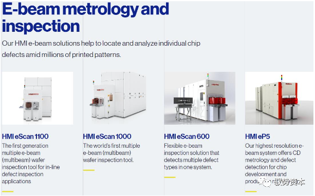
Compared to optical defect detection equipment, although electron beam detection equipment has superior performance, its point-by-point scanning method results in a slow detection speed that cannot meet the throughput requirements of wafer fabs, making it unable to replace optical equipment for online detection tasks on a large scale. Currently, it is mainly used for the development of advanced processes, with its working mode primarily being sampling detection. The mainstream suppliers on the market include ASML (which acquired Hanmin Micro Measurement Technology) and Applied Materials.
Figure: ASML HMI Series Electron Beam Pattern Wafer Defect Detection System
Source: ASML Official Website, Founder Securities Research Institute
Non-pattern wafer defect detection equipment: Its function is to detect defects in bare wafers, laying the foundation for subsequent patterned detection. Non-pattern wafer surface detection systems can detect defect types including particle contamination, pits, watermarks, scratches, shallow pits, epitaxial stacking, CMP protrusions, crystal pits, slip lines, etc., with application areas mainly falling into three categories: (1) Chip manufacturing: including incoming quality inspection, process control, wafer backside contamination detection, equipment cleanliness monitoring, etc.; (2) Wafer manufacturing: including defect detection during process development and final inspection processes before wafer shipment; (3) Semiconductor equipment manufacturing: including defect detection during process development and quality assessment of equipment processes (particles, metal contamination), etc.
The detection process: Non-pattern wafer defect detection equipment can count defects on the wafer surface, identify the types of defects, and determine their spatial distribution. By illuminating the wafer surface with a single wavelength light beam and using an optical system with a large collection angle, it collects scattered light signals from defects on the wafer surface during high-speed movement. Through multi-dimensional optical modes and multi-channel signal acquisition, it can identify wafer surface defects in real time, classify defect types, and report defect locations.
Figure: Non-pattern Wafer Defect Detection Process
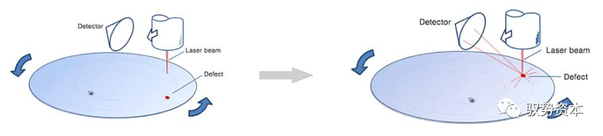
Source: Hitachi High-Tech Official Website, Founder Securities Research Institute
Dark field non-pattern detection: In optical defect detection, dark field scattering technology is commonly used for surface defect detection of precision components like wafers, with numerous advantages such as non-contact, non-destructive, high sensitivity, and fast detection speed. Compared to bright field detection, dark field detection is faster and more suitable for high-frequency three-dimensional morphology, and can detect defects much smaller than the system’s resolution and optical size, making it particularly suitable for non-pattern wafer defect detection.
Figure: Typical Dark Field Scattering Diagram and Different Defect Scattering Diagrams
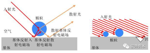
Source: “Development of Non-pattern Wafer Surface Defect Detection System Based on Dark Field Scattering”, Founder Securities Research Institute
The minimum sensitivity and throughput are key indicators. Minimum sensitivity indicates the smallest diameter of defects that the equipment can detect on the wafer surface. The smaller the value of this indicator, the better the equipment can detect smaller defects on the wafer surface. Throughput indicates the number of wafers that the equipment can detect in a unit of time. The larger the value of this indicator, the faster the detection speed of the equipment.
3. Measurement and Detection Continues to Upgrade, One of the Main Tracks for Front-end Equipment
In 2024, global wafer fab equipment spending is expected to recover to $97 billion. According to SEMI’s latest global semiconductor equipment forecast report, the global semiconductor equipment sales market size is expected to decline by 18.6% from $107.4 billion in 2022 to $87.4 billion in 2023, and then recover to over $100 billion in 2024. The decline in the market size in 2023 is mainly due to weak chip demand and increased inventory of consumer and mobile terminal products. The recovery in market demand in 2024 is mainly attributed to the end of semiconductor inventory adjustments and the growth in semiconductor demand in the fields of high-performance computing (HPC) and automotive.
Front-end equipment remains the main driving force for industry rebound. By segmenting the equipment based on their stages, the wafer fab equipment market size is expected to decline by 18.8% year-on-year to $76.4 billion in 2023, and will be the primary driver for the overall equipment market returning to $100 billion in 2024, with the wafer fab equipment market size expected to reach $87.8 billion. In the backend equipment market, due to challenges from the macroeconomic environment and overall weak semiconductor industry demand, the semiconductor testing equipment market is expected to decline by 15% year-on-year to $6.4 billion in 2023 (expected to grow by 7.9% year-on-year in 2024), and packaging equipment is expected to decline by 20.5% year-on-year to $4.6 billion (expected to grow by 16.4% year-on-year in 2024).
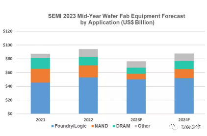
Demand for advanced process equipment remains stable, while the storage equipment market is highly volatile. Among wafer manufacturing equipment, by application field, the equipment market used for foundries and logic factories is expected to decline by 6% year-on-year to $50.1 billion in 2023, remaining the highest application field in the semiconductor equipment industry. Demand for advanced process equipment is expected to remain stable, while equipment demand for mature nodes is expected to decline slightly, with an investment scale expected to grow by 3% in 2024. Due to weak demand in both consumer and enterprise markets, the DRAM equipment market is expected to shrink by 28.8% to $8.8 billion in 2023, but as the market gradually recovers, SEMI expects this market to grow by 31% to $11.6 billion in 2024. The NAND equipment market is expected to shrink significantly by 51% to $8.4 billion in 2023, but is also expected to grow strongly by 59% to $13.3 billion in 2024.
Figure: Global Semiconductor Equipment Market Size by Segment (in $100 million)
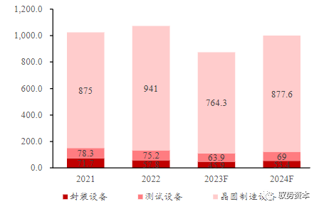
Figure: Global Wafer Manufacturing Equipment Market Size by Application (in $1 billion)
Source: SEMI, Founder Securities Research Institute
Mainland China is expected to lead the global semiconductor equipment market in 2024. By region, mainland China, Taiwan Province, and South Korea dominate the global equipment market. Among them, SEMI expects mainland China to lead the global market size in 2024, and we also see that in recent years, the share of mainland China in the global semiconductor equipment market has been on the rise, highlighting the increasing importance of the mainland equipment market.
Figure: The Increasing Importance of Mainland China’s Equipment Market (Left Axis: $1 Billion)
Source: Wind, Founder Securities Research Institute
The semiconductor equipment industry shows significant cyclicality, largely influenced by changes in the capital expenditure rhythm of downstream manufacturers. In 2017, the substantial capital expenditure by memory manufacturers drove enormous demand for semiconductor equipment, and this momentum continued into the first half of 2018. However, subsequent overcapacity led to a drop in memory prices, causing DRAM and NAND manufacturers to postpone equipment orders. The overcapacity in memory continued until the first half of 2019, and while the overall semiconductor industry was not performing well in the first half of the year, the latter half saw a recovery in industry prosperity, with wafer fabs represented by TSMC significantly increasing capital expenditures to ramp up production, although the overall demand for semiconductor equipment still fell by about 2% year-on-year in 2019. In 2020, the global semiconductor industry was impacted by the pandemic, but capital expenditures in the memory industry recovered, and strong demand in downstream sectors driven by digitalization and 5G led to a 19% year-on-year growth in the equipment market for the year. With a new round of capital expenditures initiated by semiconductor manufacturers, the global equipment market continued to grow significantly by 44% in 2021. Currently, leading overseas equipment companies like Applied Materials and Lam Research expect the global equipment market size to continue to grow in 2022.
Figure: Cyclical Growth Rate of the Semiconductor Equipment Market
Source: Wind, Founder Securities Research Institute
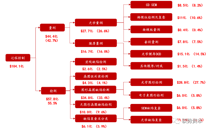
The global semiconductor equipment total market share for process control is about 10.5%, with ongoing upgrade demands. In 2021, the global process control equipment market space was about $10.4 billion, with demand for lithography-related (overlay error measurement, mask measurement and inspection, etc.) accounting for about $2.8 billion, defect detection demand for about $5.8 billion, and film thickness measurement demand for about $1.7 billion. The process control market accounts for about 10.5% of the total global semiconductor equipment market (including wafer manufacturing and packaging testing equipment), remaining relatively stable, with increasing demands for measurement and detection as wafer manufacturing processes continue to shrink and 3D stacking advances, and precision requirements continue to rise, leading to ongoing upgrade demands for process control equipment.
Figure: Global Process Control Market (in $100 million)
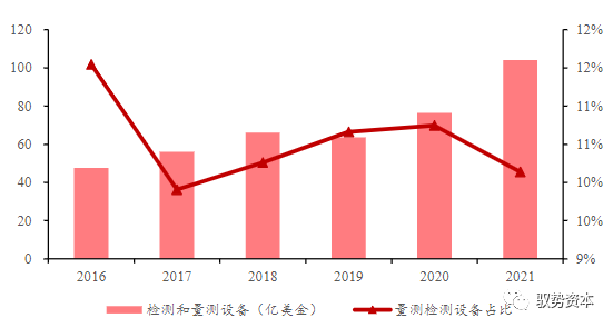
Source: VLSI, Zhongke Feicai Prospectus, Gartner, Wind, Founder Securities Research Institute
Disclaimer: This article is purely for practical discussion purposes, and the copyright belongs to the original author and related rights holders. The views represent the author’s personal opinion. If there are any issues, please contact us, and we will handle them promptly.