1. Introduction to PCB Materials
(1) Concept, Function, and Background of Printed Circuit Boards
1. The English term for printed circuit board: Printed Circuit Board
2. The abbreviation for printed circuit board: PCB
3. The main functions of printed circuit boards: Supporting circuit components and interconnecting circuit components, namely the two main roles of support and interconnection.
4. PCBs were born in the 1940s and 1950s, developed in the 1980s and 1990s. With the advancement of semiconductor technology and computer technology, printed circuit boards have developed towards high density, fine wires, and more layers, and their design technology has evolved from initial manual drawing to computer-aided design (CAD) and electronic design automation (EDA).
(2) Classification of PCBs (Copper Clad Laminates)
Definition of Copper Clad Laminate
a. Copper Clad Laminate: The English abbreviation is CCL, and it is the most basic material for making circuit boards, consisting of a laminate with one or two sides covered with metal copper foil.
b. Copper clad laminates are divided into rigid and flexible types.
c. The substrate of copper clad laminate is a non-conductive insulating material.
d. Copper clad laminate is a laminated product formed by copper foil/bonding resin/paper or fiber cloth under heat and pressure.
(2) Classification of PCBs (Copper Clad Laminates) – Single-sided boards
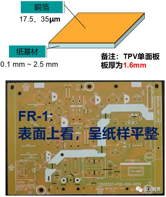
1. Paper-based phenolic resin – paper board:
a. Composition characteristics: Made by laminating paper scraps with phenolic resin, appearing flat like paper on the surface.
b. Includes: FR-1, FR-2, FR-3, XBC, HB
(Currently, TPV often uses FR-1/FR-2, FR-1 is more for MNT, FR-2 is more for TV, FR-2 has higher electrical performance requirements and higher prices, but other performance differences are not significant).
c. Advantages: Low raw material cost, as it is relatively soft, it can be punched, thus reducing processing costs in the circuit board manufacturing process.
d. Relatively poor hardness, easily absorbs moisture in humid environments, and has significant changes in thermal expansion and contraction under high temperatures, with electrical performance lower than that of fiber boards. (Example: easily deformed when passing through wave soldering)
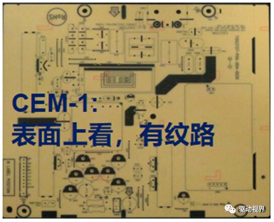
2. Paper-based epoxy resin – composite fiber board:
a. Composition characteristics: The substrate is made by mixing paper scraps and epoxy resin, with a glass fiber surface, laminated together, and appears textured on the surface.
b. Includes: CEM-1 (paper core), CEM-3 (glass fiber core). (Currently, TPV often uses CEM-1)
CEM-1 composition: copper foil + paper (core) + epoxy resin (core) + glass fiber cloth (surface)
CEM-3 composition: copper foil + glass fiber non-woven (core) + epoxy resin (core) + glass fiber cloth (surface)
CEM-3 contains more layers of fiber than CEM-1, thus its flame resistance, insulation, and hardness are higher than that of CEM-1, and it can be used to replace FR-4 for some double-sided and multilayer boards.
c. Advantages: Composite fiber boards are cheaper than glass fiber boards and solve the problems of insufficient hardness of paper boards and the difficulty of punching fiber boards.
d. Disadvantages: Although the electrical performance is close to that of glass fiber boards, it cannot completely replace FR-4 materials; only some less demanding circuit boards can use this material instead of FR-4.
(2) Classification of PCBs (Copper Clad Laminates) – Double-sided boards, Multilayer boards
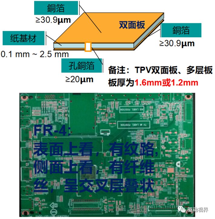
1. Glass fiber cloth-based epoxy resin – glass fiber board:
a. Composition characteristics: The substrate is made by mixing glass fiber cloth and epoxy resin, with the surface also being glass fiber cloth, laminated together, and appears textured on the surface, with fibers visible on the side, in a cross-laminated structure.
b. Includes: FR-4, etc. (Currently, TPV uses FR-4 for both double-sided and multilayer boards)
c. Advantages: High strength, heat and fire resistance (will not burn), corrosion resistance (not easily corroded, resistant to mold), moisture resistance, thermal properties (low expansion coefficient, high thermal conductivity), electrical properties (non-conductive, insulating)
d. Disadvantages: High cost, high manufacturing process requirements (e.g., cannot be punched).
2. Ceramic and metal materials: such as iron-based, aluminum-based, copper-based, mainly used in military and aerospace fields.
(2) Classification of PCBs (Copper Clad Laminates) – Material Identification
PCB material coding rules Article 34:

Special requirement code third digit represents the material used: 1 – FR-1; 2 – FR-2;
3 – CEM-1; 4 – FR-4 double-layer board; 5 – FR-4 four-layer board; 6 – FR-4 six-layer board; 7 – FPC (flexible board)
Example: 715G5713-M01-000-005K Material used: FR-4 four-layer board
(2) Classification of PCBs (Copper Clad Laminates) – Surface Treatment
1. OSP Process: OSP stands for Organic Solderability Preservative, and its process principle is a chemical reaction between an active component derived from imidazole and the surface of metal copper, forming a uniform, very thin, transparent organic coating on the solder pads and through holes of the circuit board. This coating has excellent heat resistance, with a typical thickness of 0.2-0.5μm.
(Currently, TPV requires OSP thickness to meet the requirements of two reflow soldering and one wave soldering. Manufacturers can achieve 0.2~0.35μm) During soldering, the protective film decomposes, evaporates, and dissolves into the solder paste or acidic flux, exposing the copper surface, allowing the solder to react with clean copper. Due to its low production cost and mature technology, it is now widely used.
(2) Classification of PCBs (Copper Clad Laminates) – Surface Treatment
2. Advantages and Disadvantages of OSP Process and Applications
a. Advantages: Flat, inexpensive, OSP is only compatible with copper surfaces and does not adhere to other surfaces such as solder masks, making it widely applicable.
b. Disadvantages:
① Short shelf life, under vacuum packaging conditions, the shelf life is 3 months. During storage, it should not come into contact with acidic substances, and the temperature should not be too high, otherwise, it will evaporate.
② Difficult to detect, colorless and transparent.
③ OSP itself is insulating; imidazole-based OSP, which forms a thicker coating layer, can affect electrical testing and cannot be used as a coating for electrical contact surfaces such as gold fingers, keyboard keys, and test points.
④ Cannot undergo multiple reflow soldering, generally limited to 3 times, which needs to be considered in double-sided reflow soldering and repair. After several generations of improvements, its heat resistance, storage life, and compatibility with flux have greatly improved.
⑤ The soldering temperature is relatively raised to 225℃, and a stronger (acidic) flux must be added during soldering to eliminate the protective film, otherwise, it will lead to soldering defects.
Source: Compiled by JXPCA.
Copyright statement: The copyright of this article belongs to the original author and does not represent the views of the association. The articles promoted by the “Jiangxi Province Electronic Circuit Industry Association” are shared for reference only and do not represent the position of this account. If there are copyright issues, please contact us for deletion.
Welcome to submit articles, soft texts, and advertising cooperation
Miss Ouyang: 18827872107
JXPCA