Source: WeChat Official Account “Semiconductor Industry Watch”
With the rapid development of consumer electronics and large-scale data centers driven by technologies such as 5G, AI, and IoT, the market demand for storage will become increasingly intense.
As one of the important types of semiconductor products, memory accounts for about one-third of the global semiconductor market value. Data shows that global memory revenue increased by $13.5 billion in 2020, accounting for 44% of the total revenue growth of the semiconductor market in 2020.
Overview of the Memory Market
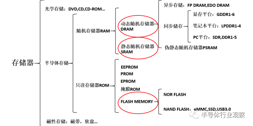
From the perspective of market size, the most mainstream memory types currently are DRAM, NAND Flash, and NOR Flash, which together account for about 95% of all semiconductor memory, especially the first two, which account for about 90% of the total, with market sizes in the hundreds of billions of dollars.
Basic Types of Memory: Source – Wikipedia, Changjiang Securities Research Institute
Among them, the market size of DRAM reached $100 billion in 2018. According to the latest forecast from IC Insights, the global DRAM market size is expected to reach about $121.9 billion by 2026. Compared to DRAM and NAND, the market for NOR Flash is much smaller, with a global scale of about $3 billion, and is also more fragmented.
Semiconductor memory is a highly monopolized market, with DRAM and NAND Flash basically dominated by the top three companies, and the degree of monopoly has gradually intensified in recent years. According to data from the Chinese flash memory market, in 2020, 95% of the DRAM market share was occupied by Samsung, SK Hynix, and Micron, while Samsung, Kioxia, Western Digital, Micron, SK Hynix, and Intel accounted for about 99% of the NAND market.
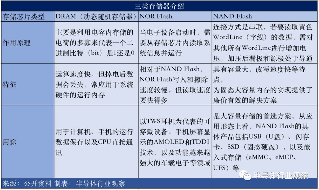
Specifically looking at these three major types of memory, they each have their differences:
DRAM is volatile, with small capacity. Although DRAM has excellent performance in many aspects—nanosecond-level latency, bandwidth of tens of GB/S, and a lifespan close to “immortality”; however, it is a volatile memory, meaning data will be lost after power off, and its cost is higher than flash memory, with a smaller capacity.
NAND Flash has long latency, short lifespan, and planar miniaturization has reached its limits. Each time data is written, high voltage needs to be applied to allow electrons to break through the oxide film of the transistor and enter the floating gate, which causes irreversible damage to the oxide film. The best-performing SLC NAND has a read/write cycle of only about 100,000 times, while lower-performing MLC and TLC have read/write lifespans on the order of thousands.
NOR Flash features Execute In Place (XIP), meaning applications do not need to read code into system RAM, but can run directly in Flash memory, thus achieving high transmission efficiency and fast read speeds, with high cost-effectiveness at small capacities of 1-4MB, mainly used for program storage. However, the device structure of NOR requires that all bits be written to 0 before erasing, which results in low erase speeds, and since Flash requires erasure before writing data, this also affects the write speed of NOR.
In summary, these three mainstream memory types have their respective advantages and disadvantages, and as technology advances, their shortcomings are gradually magnified.
Existing Storage Technologies Face Huge Challenges
Small cell size, high performance, and low power consumption have always been the goals pursued by memory manufacturers.
As semiconductor processes move below 14nm and migrate to Fin-FET (Fin Field-Effect Transistor), this technology cannot be directly applied to some existing embedded memory elements. Furthermore, the future demands for high computing power from artificial intelligence (AI) and edge computing make the high power consumption and speed issues of existing high-capacity memories, such as DRAM and NAND flash, unable to keep up with demand.
As memory density continues to increase, basic component sizes continue to shrink, and CPU demands for memory capacity continue to grow, these problems will become increasingly severe in the future.
The core of semiconductors is Moore’s Law, which simply states that by making unit components smaller, the storage density and functionality on a single wafer are increased. Existing storage technologies (DRAM and Flash) face the same problem—semiconductor process miniaturization cannot continue to shrink.
At the same time, memory consumes too much power. IoT and mobile devices operate on battery power, and their memories must be carefully selected because they consume a significant portion of battery power, reducing battery life.
The next generation of mobile architectures will introduce higher computing power requirements for AI and edge computing, while requiring lower power consumption to meet consumer expectations and win in a tough market competition. Of course, all of this must be achieved at a low cost, which is the challenge faced by existing storage technologies.
In summary, existing memory has issues such as performance mismatch between internal and external storage, non-volatility of internal memory, and difficulties in shrinking external storage, thus new types of memory are gaining widespread attention. Industry insiders point out that new storage technologies will inevitably replace existing storage technologies, which is an inevitable trend in historical development.
What Problems Can New Types of Storage Solve?
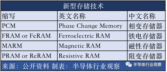
Currently, popular new types of storage technologies mainly include MRAM, ReRAM, PRAM, and FeRAM.
PCM (Phase Change RAM):Phase Change RAM, this type of memory utilizes the difference in conductivity between the crystalline and amorphous states of materials to store information, with the process mainly divided into SET and RESET.
FRAM (Ferromagnetic RAM):Ferroelectric RAM, structurally similar to DRAM, with basic units consisting of a MOS transistor and a capacitor, but the dielectric material of DRAM’s capacitor cannot continue to store charge after power off, whereas FRAM uses ferroelectric crystals that do not lose charge when powered off as the dielectric. When voltage is applied to the planar capacitor, the ferroelectric crystal forms polarized charge under the electric field, with lower polarized charge formed under positive voltage and higher polarized charge under negative voltage. This binary stable state allows it to function as memory.
MRAM (Magnetic RAM):Magnetic Random Access Memory, which stores data through magnetic polarization rather than charge.
ReRAM (Resistive Random Access Memory):Resistive Random Access Memory, a typical ReRAM consists of two metal electrodes sandwiching a thin dielectric layer, with the dielectric layer serving as the medium for ion transport and storage.
These new types of memory either have faster access speeds, higher durability, smaller die sizes, lower costs, and power consumption, or may even support the development of in-memory compute in the future.
The emergence of new storage technologies can solve the power consumption issues of mainstream memory today. Additionally, these new types of memory are all non-volatile, so they do not need to be refreshed.
Compared to DRAM, new storage technologies can automatically reduce power consumption by 20%. Since they can overwrite old data without erasure, they save the high erase energy required for flash memory, as well as the delays caused by slow erase cycles (this property is called In-Situ Programming).
Compared to flash memory, these new technologies have very low energy requirements for the writing process, reducing or eliminating the need for inefficient charge pumps. Finally, all these new technologies provide random data access, reducing the need to maintain two copies—one in flash memory and one in DRAM.
Therefore, using new storage technology to replace today’s traditional DRAM + NAND flash architecture will bring significant power savings and performance improvements.
Currently, new types of storage are still in their infancy, with PCM (Phase Change Memory) technology being the most mature and the only one with large capacity and mass production capabilities.
PCM (Phase Change Memory), also known as PRAM (Phase-change RAM), has a research history of several decades. Intel co-founder Gordon Moore published a paper describing early prototypes as early as 1970: Phase Change Memory stores data by changing the phase of materials through thermal energy, switching between low-resistance crystalline (conductive) state and high-resistance amorphous (non-conductive) state.
PCM is slower than DRAM but nearly 1000 times faster than Flash; its storage density is higher than DRAM but lower than Flash. In current memory applications, DRAM and Flash are mismatched in the overall system, requiring new memory to build the entire architecture. PCM has many advantages, and there is significant market demand, with many companies promoting its industrialization process.
Samsung produced a 512Mb phase change memory chip based on 90nm technology in 2008; a 1Gb chip based on 58nm technology in 2011; and an 8Gb chip based on 20nm technology in 2012; and released an industrial report on phase change memory in 2014.
Micron produced a 1Gb phase change memory chip based on 45nm technology in 2009; released the first SSD based on phase change memory in 2011; achieved mass production of a 1Gb phase change memory chip based on 45nm technology in 2013; and in 2015 jointly released 3D Xpoint with Intel.
STMicroelectronics jointly released a 4Mb embedded phase change memory chip based on 90nm technology with Hengyi in 2009; released a paper in 2010 on achieving better thermal stability and data retention through material modification engineering N-GeTe; and in 2013 released a paper on achieving performance balance between SET and high/low retention through material modification engineering N-Ge-GST.
IBM released multi-value phase change memory operation algorithms in 2011, then launched multi-layer crosspoint memory based on MIEC materials. In 2014, IBM released solutions for multi-value memory resistance drift algorithms, and in 2016 launched multi-value phase change memory, entering the 90nm process. Other international manufacturers, including Intel and TSMC, have also done related work.
China’s new storage industrialization capabilities and intellectual property layout are still in their infancy. The patents for phase change memory and resistive memory began to gradually increase around 2000, while magnetic memory has relatively earlier patent applications, starting in 1990.
Since 2002, the Shanghai Institute of Microsystems, Chinese Academy of Sciences has begun tackling the next generation of new phase change memory, undertaking relevant tasks such as China’s “Large Scale Integrated Circuit Manufacturing Equipment and Complete Technology” and “973 Plan.” In 2011, the Shanghai Institute of Microsystems, SMIC, and Microchip formed a research and development team of more than 100 people, successfully developing phase change memory with independent technology, and then further developing it into the engineering field.
It is worth noting a domestic manufacturer—Jiangsu Times Semiconductor (hereinafter referred to as “Times Semiconductor”), which has been conducting PCM research and development for over 10 years, is currently the only semiconductor company in China that has truly formed PCM production capabilities, and is one of the few semiconductor enterprises globally with independent research and production capabilities in the fourth generation of memory.
According to reports, the company’s products have already entered mass production and are currently ramping up yield, with engineering samples passing tests from multiple customers. The first phase of the product primarily produces market-common EEPROM and NOR Flash, while the second phase focuses on producing permanent memory and high-performance flash memory.
Data shows that the total investment in Jiangsu Huai’an PCM production project is 13 billion yuan, with an initial investment of 4.3 billion yuan, which settled in the national-level Huai’an High-tech Industrial Development Zone on September 28, 2016, and achieved the completion of the factory building in 9 months, with the first equipment entering the factory on March 22. Upon full completion, it will reach an annual production capacity of 100,000 12-inch phase change memory wafers, achieving sales of 4.5 billion yuan annually. Currently, the first phase has the capability to produce 60,000 wafers per year. Since the project settled in Huai’an in September 2016, Times Semiconductor has maintained a rapid project advancement speed.
Currently, China’s PCM technology development still has some distance from international giants, and it should be market-oriented, with the industry as the main body, combining existing research teams to rapidly promote the industrialization of new storage. At the same time, it should avoid blind scaling. Of course, attention should also be paid to the collaborative development of the industry’s upstream and downstream. Encouraging the integration of whole machine, CPU, and storage enterprises to participate together will help quickly shape the new storage industry chain.
Today, the storage market is dominated by storage giants such as Samsung, SK Hynix, and Micron. It is increasingly difficult for domestic manufacturers to enter this market. However, the new storage industry is not yet mature, and opportunities outweigh challenges. In terms of industry structure, compared to traditional DRAM and NAND Flash, new storage has not yet formed an industry monopoly, and the product route is not clear enough.
China has the potential to overtake in this field. Technologically, the future storage technology route is still unclear, presenting opportunities for technological catch-up or even surpassing. In the market, with the rapid development of emerging fields such as 5G and artificial intelligence in China, the demand for storage is experiencing explosive growth, creating a sufficiently broad potential market for new storage.
With the joint efforts of manufacturers like Times Semiconductor developing new storage technologies such as PCM, along with Changjiang Storage, Unisoc, and Hefei Changxin developing mainstream storage like DRAM and NAND Flash, a spark can ignite a prairie fire.
Editor: Lemon