 Click the blue text to follow, grateful for your support
Welcome friends to follow the “Hao Xushuang Electronic Design Team” public account. This account will regularly update relevant technical materials, software, etc. Friends who are interested can browse other “modules” of this public account, hoping that everyone can gain something they desire from this public account.
This article mainly discusses the understanding of logic analyzers in FPGAs
 The logic analyzer in an FPGA can be understood as “a spy implanted inside the FPGA chip, specifically designed to probe signal states.” It is fundamentally different from traditional external logic analyzers (a standalone hardware device connected to chip pins via probes).
Core Concept
The logic analyzer in an FPGA, often referred to as “on-chip logic analyzer” or “embedded logic analyzer,” is best represented by Xilinx (AMD)’s ChipScope™ and Intel (Altera)’s SignalTap™.
The core idea is to utilize the surplus logic and memory resources within the FPGA to create a miniature debugging circuit that can capture and store the internal signal states of the FPGA in real-time, and transmit the captured data to software on a computer for display and analysis via interfaces like JTAG.
In simple terms, you are using a portion of the FPGA’s resources to create a logic analyzer to debug other circuits you have designed.
Why Do We Need It?
Traditional logic analyzers (oscilloscopes, digital logic analyzers) are like using a stethoscope to listen to the heartbeat from the outside, while on-chip logic analyzers are like placing a sensor directly inside the heart.
For debugging complex digital logic, bus protocols (such as AXI, PCIe), state machines, etc., it is anirreplaceable tool.
Comparison with Traditional Logic Analyzers
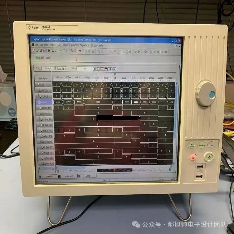
Traditional (External) Logic Analyzers
Probe Points: Can only measure signals at the external pins of the chip
Setup Method: Configured on the external device panel or software
Clock: Uses its own high-precision clock source
Bandwidth/Speed: Limited by physical connections (probes, cables), signal integrity is a challenge at high frequencies
Disadvantages: Pin count, PCB routing, probe costs
Debugging Flexibility: Can be used immediately after the design is completed and probes are connected
FPGA On-Chip Logic Analyzers
Probe Points: Signals from any register or wire inside the FPGA
Setup Method: Integrated into the design code through IP core tools in the FPGA project
Clock: Samples using the design’s own clock, perfectly synchronized
Bandwidth/Speed: Directly connected to internal nodes, extremely high bandwidth, capable of easily capturing signals in the hundreds of MHz or even GHz
Disadvantages: Consumes valuable FPGA resources (logic units, block RAM, routing resources)
Debugging Flexibility: Requires recompilation, layout, and routing, and downloading a new FPGA configuration file
Working Principle
Instrumentation:
In your HDL code (Verilog/VHDL), mark the signals (nets) you want to observe.
In EDA tools (such as Vivado, Quartus), use IP core insertion tools (ChipScope Pro, SignalTap Logic Analyzer) to connect these signals to the inputs of the logic analyzer IP core.
Set key parameters: sampling clock (which clock to use for data capture), sampling depth (how long of data to capture, which consumes RAM resources proportionally), trigger conditions (under what circumstances to start capturing data).
Compilation:
The tools will synthesize, layout, and route your design code along with the logic analyzer IP core, generating a new FPGA configuration file (.bit / .sof file). This file contains your functionality and debugging circuit.
Trigger & Capture:
Download the new configuration file to the FPGA to run.
The logic analyzer circuit silently monitors the specified signals in real-time alongside your design.
Once the set trigger conditions are met (for example, a state machine enters the “ERROR” state, or a specific address write operation occurs on the AXI bus), the logic analyzer immediately springs into action: it rapidly stores all signal data from a period before and after the trigger point into its dedicated block RAM.
Upload & Display:
After capturing is complete, the logic analyzer circuit uploads the waveform data stored in RAM to the debugging software on the computer via the FPGA’s JTAG interface.
Once the software receives the data, it displays it in a waveform format similar to that of traditional logic analyzers or simulations for analysis and debugging.
Key Understanding Points Summary
Resource Overhead: Using it comes at a cost (logic, RAM). The larger the sampling depth and the more complex the trigger conditions, the more resources consumed.
Recompilation: Every time you modify the signals to observe or the trigger conditions, you almost always have to re-synthesize and layout, which can be time-consuming.
Non-real-time Stream: It captures data within a time window, rather than continuously sending a data stream to the computer (which would require extremely high bandwidth that JTAG cannot meet).
Irreplaceability: For complex FPGA internal debugging, it is the most efficient and sometimes the only means.
Some resources in this article are sourced from the internet; if there is any infringement, please contact the author.
If you find this public account good, please recommend it to your friends, thank you and best wishes!