
Source: Content from Semiconductor Industry Observation (ID: icbank) translated from eejournal, thank you.
Ates Berna, General Manager and Managing Partner of ElectraIC in Istanbul, Turkey, recently published a comparative summary chart on LinkedIn, showcasing the differences between FPGA and ASIC. While this is not a detailed chart, I believe it serves as a great icebreaker when you need a fairly complex high-performance, non-standard IC to address design challenges, leading to discussions about your choice between FPGA and ASIC. I often receive questions about FPGA versus ASIC, and I think it is valuable to discuss the chart published by Berna. Therefore, here is a more detailed line-by-line discussion of the items in the chart: 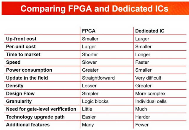 This is my line-by-line discussion of the chart: Upfront Costs: The upfront costs for ASIC are high. First, there is the cost of ASIC development tools. You need a fairly large toolchain to develop ASICs, which you must rent or purchase, and you need to know how to use these tools. If your design team lacks this knowledge, you need to include the cost of training the team in your upfront cost list. Additionally, you will incur significant NRE (Non-Recurring Engineering) costs, which can amount to hundreds of thousands or millions of dollars, paid to the silicon foundry to build your ASIC. NRE costs cover mask fabrication and inspection, reserving a spot in the foundry’s busy manufacturing schedule to produce your ASIC, chip testing and sorting, packaging, and final testing. In contrast, FPGAs are off-the-shelf components, so there are no foundry NRE costs, and FPGA tools are much cheaper than ASIC design tools, typically lower by three orders of magnitude. Depending on the FPGA, you can even purchase parts through distribution and receive them the next day. Unit Cost: This is where ASIC shines. Because you typically design ASICs to meet your exact design requirements, you only purchase the silicon you truly want. There is little to no waste. Therefore, assuming you have projected product sales to justify creating an ASIC, the unit cost of ASIC should be lower than that of FPGA. This is because FPGAs have a significant chip overhead. First, your design may not fully utilize any given FPGA. If you’re lucky, you might achieve 90% utilization. Typically, you may not be able to use up to 10% or more of the FPGA resources to meet routing and timing goals due to excessive routing congestion, and if you try to use the entire FPGA, signals may become too long and slow. Additionally, the signal routing matrix on an FPGA is very rich to ensure you can route your design on the FPGA. Time to Market: So far, FPGAs are the leaders in time to market. If you are ready to manufacture the PCB, you can ship on the same day the FPGA design is completed. All you need to do is flash the final configuration into the EEPROM on the board, test it, package it, and ship it. In contrast, when you finish the ASIC design, you send the design to the silicon foundry and hold a tape-out party. Then, you wait for months while the foundry accepts your design, inspects it, manufactures the chips, tests the chips, packages the chips, and then sends the packaged ASIC back to you. When you receive the completed ASIC box, you can build and test your circuit board. Meanwhile, similar products from competitors, based on FPGAs, will have been on the market while you wait for the ASIC to return from the foundry. If time to market is critical for you, then FPGA may be your best choice. Speed: Assuming your designers know what they are doing, ASIC extracts the highest performance from any given IC process node. Due to the large (capacitive) programmable routing matrix of FPGAs, performance is typically lost by about an order of magnitude compared to ASICs for any given IC process node. Power Consumption: This is not obvious, but the silicon efficiency of FPGAs in terms of unit cost and speed also increases the power consumption of FPGAs relative to ASICs. All those extra routing matrix transistors on FPGAs leak, leading to higher static power consumption. The inherent longer routing in FPGAs, due to the Manhattan routing required in structured FPGAs, adds capacitance for each routing, resulting in higher dynamic power consumption. However, FPGA vendors can counteract the extra power consumption in their FPGAs. For example, Lattice Semiconductor chose a 28nm FDSOI process technology for its Nexus FPGAs to reduce static power consumption. There are many such design techniques to reduce power consumption, but FPGAs have large chips, and large chips have a lot of capacitance. Field Updates: This is easy to understand. SRAM-based FPGAs are easy to reprogram in the field. Change the configuration stored in flash memory and update your design. In the early days of FPGA design, you had to pull the old configuration EPROM or EEPROM from its IC socket and insert a new configuration to perform a field update. Nowadays, you are likely to perform reprogrammable designs via USB or JTAG ports. Some end product designs allow for wireless updates, although there are many security issues associated with allowing wireless hardware updates. In contrast, updating an ASIC typically requires a board swap (known as a service call in the wireless industry). Some ASIC designs incorporate embedded FPGA (eFPGA) structures from eFPGA vendors (such as Achronix, Flex Logix, Menta, or QuickLogic) to allow for a limited number of field updates without a service call. If you want to adopt this approach, you can even obtain an open-source FPGA structure generator and toolset called OpenFPGA. However, if you embed FPGA architecture in an ASIC, doesn’t that make the ASIC an FPGA?Density: Because device density is closely related to unit cost, the same argument applies to FPGA versus ASIC, just with a little more nuance. In any given process technology, due to the routing overhead and resource utilization limitations of FPGAs, you can always design a larger device, an ASIC with more resources, as mentioned above. Design Process: Unlike ASICs, the physical design of FPGAs is completed and verified by the FPGA vendor before you see the device, although there are errata. You typically use a vendor’s toolchain to design the FPGA configuration, although some wealthy design companies use ASIC-level layout and routing tools from one of the three major EDA vendors: Cadence, Siemens/Mentor, and Synopsys. For ASIC design, you typically take a mixed approach, purchasing EDA tools from the three major EDA companies, and perhaps also buying some additional design tools from new EDA startups that have not yet been absorbed by one of the three major EDA companies. Granularity: The digital granularity of ASICs is a gate, or in some cases, a transistor. FPGAs must have coarser granularity, around a logic element. Otherwise, the routing overhead of FPGAs would become completely impractical. This difference in granularity between ASICs and FPGAs leads to higher unit costs for FPGAs and a relative lack of density. Gate-Level Verification Requirement: Both FPGAs and ASICs require design-level verification. However, FPGAs are not gate-level fine-grained, so they do not require gate-level verification. You place each gate in an ASIC design, so you need to verify each gate. Technology Upgrade Path: In theory, upgrading from one FPGA series to the next within a vendor’s product line is easier. For example, migrating designs through three Xilinx 7 series devices: Artix, Kintex, and Virtex is relatively straightforward. However, migrating to FPGAs from other vendors also means migrating to the design tools of other FPGA vendors, which is not particularly easy, although it is not as difficult as some might think. Engineers have managed to master the toolchains of more than one FPGA vendor. They just complain a lot when making the change. ASICs do not have a technology upgrade path. To upgrade an ASIC, you need to design, verify, and manufacture a new ASIC. Additional Features: Here, I must differ from the chart above. While FPGA vendors have long sought to add additional feature blocks to their FPGAs, almost anything available on FPGAs can be designed or purchased as IP and placed on an ASIC. This may not be easy, but it is usually possible. Claims about ASIC IP include embedded FPGA IP. Perhaps the chart is intended to indicate that it is easier to leverage many other cutting-edge features that FPGA vendors have crammed into their parts. For example, FPGA vendors have been leading high-speed SerDes design for the past 20 years. If you want a fast SerDes, you are likely to find the fastest on the latest devices from FPGA vendors, especially Achronix, Intel, and Xilinx. Of course, there are many other design considerations that did not appear in the chart above. For instance, there is an intermediate step between FPGAs and ASICs—structured ASICs—which offer many (but not all) of the advantages of ASICs at a lower NRE cost compared to ASICs. Fifteen years ago, many companies offered structured ASICs and suggested they were the next generation of gate arrays. For many commercial reasons, only one commercial structured ASIC vendor remains—Intel, which acquired the last structured ASIC vendor, eASIC, in 2018. Although the chart that triggered this article is not comprehensive, it does provide a good starting point for making decisions between FPGA and ASIC. By now, this article should have struck a chord with someone, so feel free to comment and let us know your thoughts.