1 I2C Bus
The programming related to I2C mainly involves two situations: ARM chips with dedicated controllers and microcontroller chips without controllers. For ARM chips with controllers, operations are performed based on the data manual by setting the corresponding registers (control registers, status registers, etc.); however, for microcontroller chips without controllers, I2C protocol needs to be simulated through the corresponding pins.
First, let’s discuss the I2C protocol. The signals involved can be divided into three categories: start signal, stop signal, and data transmission. Since it is a protocol, it is a set of rules agreed upon by both parties in advance, and the communication parties can transmit data according to this standard. To ensure the consistency of data transmission, additional check information may be sent at certain times, such as ACK signals and non-ACK signals.
Start Signal: When SCL is high, SDA transitions from high to low, indicating the start of data transmission.
Stop Signal: When SCL is high, SDA transitions from low to high, indicating the end of data transmission.
ACK Signal: The receiving IC sends a specific low-level pulse to the sending IC after receiving 8 bits of data, indicating that the data has been received. After the CPU sends a signal to the controlled unit, it waits for the controlled unit to send an ACK signal. Upon receiving the ACK signal, the CPU determines whether to continue transmitting signals based on the actual situation. If no ACK signal is received, it is judged that the controlled unit has failed.
To simulate I2C signals based on microcontrollers, the above timing must be strictly followed in the research and implementation.
Next, let’s look at the I2C control of ARM chips with I2C controllers, such as s3c2410 and s3c2440. This mainly includes the settings of four related registers: through their mutual cooperation, I2C data transmission is realized.
IICON: Control register. It is mainly used to control whether to send ACK signals, set the clock for the transmitter, enable I2C interrupts, and indicate whether interrupts have occurred.
IISTAT: Status register. It selects the I2C working mode, sends S signals, P signals, enables receive/send functions, and indicates various statuses, such as whether bus arbitration was successful, whether it was addressed as a slave, whether it received address 0, and whether it received ACK signals.
IICADD: Multi-master I2C address register;
IICDS: Data shift register for sending and receiving;
Next, according to the data manual, we will write the corresponding code based on the workflow of its host sender.
Three functions can implement a simple I2C protocol: read, write, and interrupt;
The programming idea is as follows:
The write function and read function simply start the I2C transmission and then wait until the data is fully transmitted in the interrupt service routine before returning.
2 Understanding SPI Protocol (CPOL and CPHA in SPI)
[Background]
Recently, I was looking at some driver code for Silicon Labs’ C8051F347, particularly the initialization code for the SPI part, and saw that its SPI settings were CPOL=1, CPHA=0. Not understanding the meaning of CPOL and CPHA, I wanted to figure out what these two parameters really mean and why they are set this way. Therefore, I searched for relevant information on SPI polarity and phase, and summarized it as follows.
[Introduction to Basic SPI Knowledge]
Devices communicate with each other through some hardware interface, and there are many types of interfaces, with SPI being one of them.
In SPI, there are Master and Slave devices, and data transmission is controlled by the Master.
A master can connect to one or more slaves.
The common usage is to connect one Master to one Slave, requiring only four wires:
SCLK: Serial Clock;
MISO: Master In Slave Out;
MOSI: Master Out Slave In;
SS: Slave Select;
Because SPI has a relatively simple interface (only requiring four wires), it is widely used, mainly in communication between EEPROM, FLASH, real-time clocks, AD converters, digital signal processors, and digital signal decoders. That is, an SPI Master communicates with a Slave device, such as those mentioned above, like Flash and ADC.
For communication between master and slave devices via SPI, it is first necessary to ensure that the clocks (SCLK) of both are consistent; they must agree on this to match; otherwise, normal communication cannot occur, meaning that timing consistency is necessary for normal communication. The clock and phase in SPI refer to the characteristics of the SCLK clock, ensuring that the clock characteristics of both master and slave devices match to enable normal SPI communication.
[Common Abbreviations or Terms Related to SPI]
First, let’s briefly discuss some common terms in SPI:
SPI’s polarity and phase are most commonly referred to as CPOL and CPHA, but there are also some other notations. A simple summary is as follows:
(1) CKPOL (Clock Polarity) = CPOL = POL = Polarity;
(2) CKPHA (Clock Phase) = CPHA = PHA = Phase;
(3) SCK=SCLK=SPI Clock;
(4) Edge = the moment when the clock level changes, either rising edge or falling edge;
For one clock cycle, there are two edges, referred to as:
Leading edge = the first edge; if the starting voltage is 1, then it is when it changes from 1 to 0; if the starting voltage is 0, then it is when it changes from 0 to 1;
Trailing edge = the second edge; if the starting voltage is 1, then it is when it changes from 0 to 1 (i.e., after the first 1 changes to 0, the subsequent 0 can change to 1); if the starting voltage is 0, then it is when it changes from 1 to 0;
This article uses the following notations:
Polarity = CPOL
Phase = CPHA
SCLK = Clock
First edge and second edge
[SPI Phase and Polarity]
CPOL and CPHA can each be 0 or 1, resulting in four combinations:
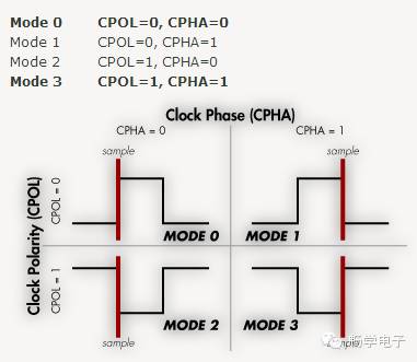
From this diagram, it is clear that polarity and phase mainly control certain aspects. When CPOL equals 0, the idle level of the clock is 0; when CPOL equals 1, the idle level is 1; and CPHA determines the moment of data sampling, whether it is at the first edge or the second edge.
[How to Understand and Remember CPOL and CPHA]
Therefore, regarding CPOL and CPHA, which seem complex and difficult to understand and remember, after the above explanation, they can be easily understood:
Look at the timing diagram; if the initial level of SCLK is 0, then CPOL=0; if it is 1, then CPOL=1.
Then look at the data sampling moment, which corresponds to the middle of the rectangular area of the data line in the timing diagram, corresponding to the position of the SCLK clock, determining whether it is the first edge or the second edge, which corresponds to CPHA being 0 or 1. (Whether it corresponds to the rising edge or the falling edge depends on the value of CPOL).
That is:
(1) How to determine CPOL: The voltage of SCLK during idle time determines whether CPOL is 0 or 1;
(2) How to determine CPHA: The moment of data sampling corresponding to SCLK is at the first edge or the second edge, corresponding to CPHA being 0 or 1.
[How to Set SPI Polarity and Phase in Software]
SPI consists of master and slave devices, which communicate via the SPI protocol.
Setting the SPI mode of the slave device determines the mode of the master device.
Therefore, it is necessary to first understand what mode the slave device’s SPI is in, and then set the master device’s SPI mode to match the slave device’s mode for normal communication.
For the slave device’s SPI mode, there are two types:
(1) Fixed, determined by the hardware of the SPI slave device
For SPI slaves, the specific mode will be described in the relevant datasheet, which needs to be found in the datasheet. For example:
Regarding the SPI slave device, whether the idle state is high or low determines whether CPOL is 0 or 1;
Then find out whether the device samples data on the rising edge or falling edge, so that, given the value of CPOL, it can be deduced whether CPHA is 0 or 1.
Example 1:
In the datasheet for the CC2500 – Low-Cost Low-Power 2.4 GHz RF Transceiver, the SPI timing diagram is:
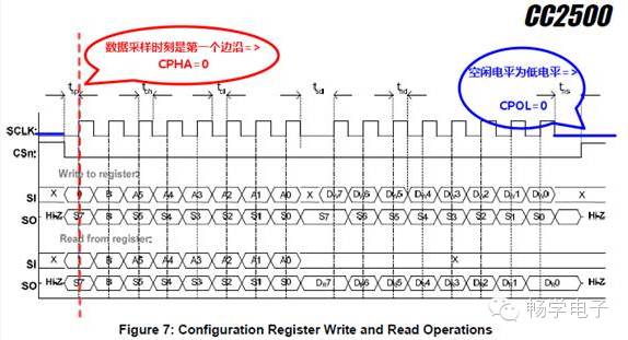
From the diagram, it can be seen that the initial SCLK and the final SCLK during idle time are low, deducing that CPOL=0. Then, at the moment of data sampling, which corresponds to the first edge of SCLK, CPHA=0 (this corresponds to the rising edge).
Example 2:
In the datasheet for the SSD1289 – 240 RGB x 320 TFT LCD Controller Driver, it states:
“SDI is shifted into the 8-bit shift register on every rising edge of SCK in the order of data bit 7, data bit 6 … data bit 0.”
This means that data is sampled on the rising edge, so it can be determined that either CPOL=0, CPHA=0, or CPOL=1, CPHA=1 mode is used, but which specific mode it is.
Logically, next we should determine whether SCLK is high or low during idle time to determine whether CPOL is 0 or 1, but the datasheet does not mention this.
So, at this point, it is unclear whether both modes are supported or if additional evidence is needed to confirm whether CPOL is 0 or 1.
(2) Configurable, set by software
The slave device is also an SPI controller, supporting all four modes, and can be set to any of those modes.
After understanding the mode of the slave device, set the master device’s mode to match the slave device’s mode for proper communication.
To configure SPI’s CPOL and CPHA, it is generally just a matter of writing the corresponding bits for CPOL and CPHA in the appropriate registers of the SPI controller, writing 0 or 1 as needed.
Example:
The SPI controller in the C8051F347 supports software configuration of CPOL and CPHA values, supporting all four modes. In this case, the C8051F347 is set as the SPI slave device with CPOL=1, CPHA=0 mode, so the corresponding master chip, Blackfin F537’s SPI controller, as the master device, must also set its SPI mode to CPOL=1, CPHA=0.
For the full text, see the original.