The I²C bus is very common in embedded systems, but recently in a group (possibly a beginner group) communication, I was quite surprised that many people do not even understand the I²C bus basics. Today, I will explain the timing of the I²C bus.
Many electronic engineers should know about the I²C bus from EEPROM communication, actually, the I²C bus is far more than just for EEPROM storage, it also has similar applications like 485, SPI, etc.
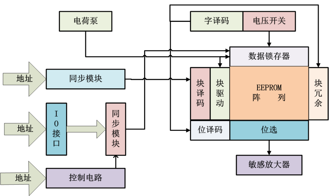
EEPROM Storage System Architecture Diagram
The I2C bus is a bidirectional two-wire synchronous serial bus developed by Philips, allowing effective control between ICs with just two wires (SDA and SCL) to transmit information between devices connected to the bus.
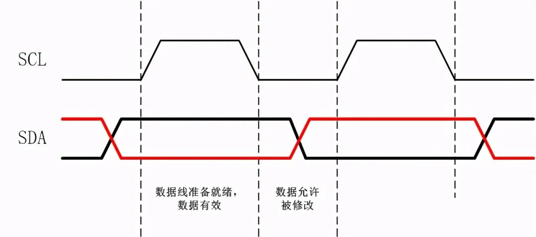
Data on the I2C bus is transmitted bit by bit. SCL is the clock line, and SDA is the data line; when SCL is high, the level on the SDA data line cannot be changed, and when SCL is low, the level on the SDA data line can be high or low.
Bit Transmission of the I2C Bus
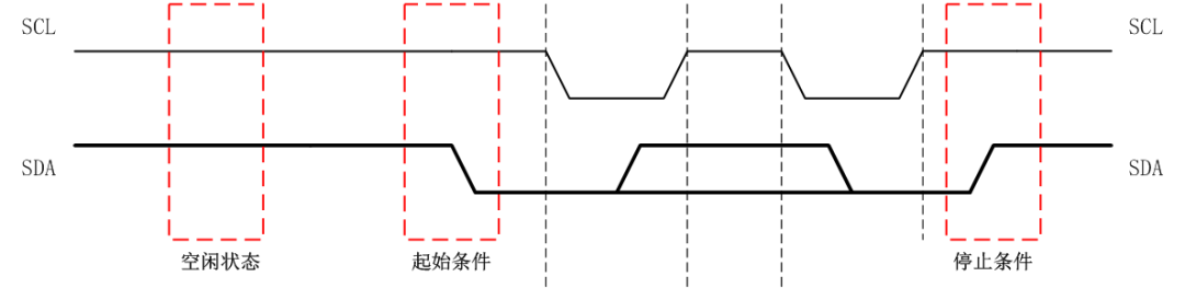
Start Condition: When SCL is high, SDA switches from high to low; indicating the start of data transmission.
Stop Condition: When SCL is high, SDA transitions from low to high; indicating the end of data transmission.
Idle Condition: Both SDA and SCL lines of the I2C bus are high; indicating an idle state.
Start and Stop Conditions
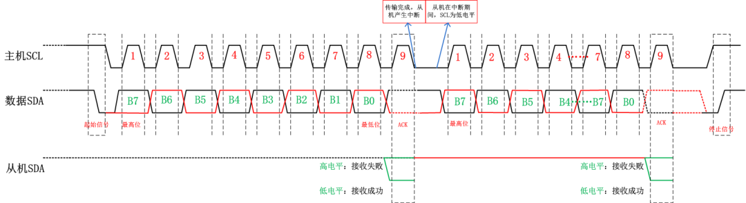
Byte Transmission
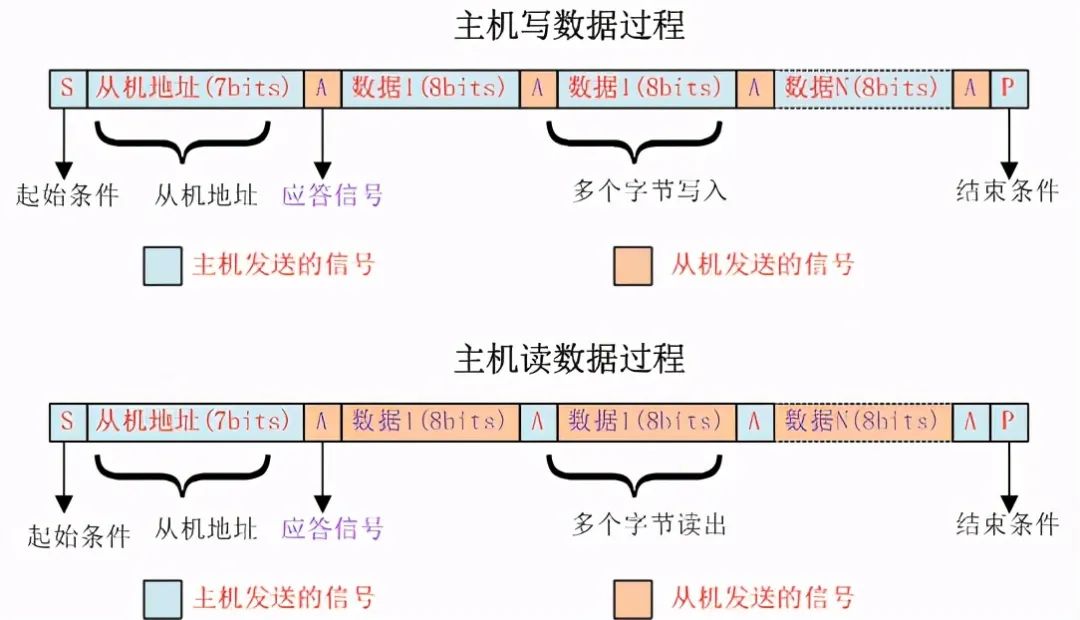
When sending data, the master first sends a start signal on the I2C bus, then switches the SDA signal to output mode, and sends out the 8-bit data from high to low sequentially;
After sending, the master switches the SDA signal to input mode, waiting for the slave to respond with ACK or NAK; then sends the next data
I2C Bus Data Transmission
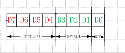
In the I2C bus system, each device has a fixed address, usually determined by the chip’s A0, A1, and A2. The slave address byte consists of seven address bits (D7-D1) and one direction bit (D0).
The D7-D4 bits of the device address are generally fixed by the manufacturer to 1111, while the remaining D3, D2, and D1 are connected to the chip’s A2, A1, and A0 to determine; D0 is 0x00 for write, and D0 is 0x01 for read. This is why you see examples like 0xA0 and 0xA1.
1. The master sends an I2C bus stop signal to prevent data write failure due to a busy bus
2. The master sends an I2C bus reset signal to ensure the bus is idle before writing data
3. The master sends an I2C bus start signal to initiate a data write
4. The master sends the I2C slave address and write mode (W/R=0) signal, and waits for a slave acknowledgment signal
5. After receiving the ACK acknowledgment signal, the master begins writing multiple bytes, needing to wait for a slave acknowledgment signal after writing each byte
6. After receiving the ACK acknowledgment signal, the master sends the I2C bus stop signal to ensure the bus is idle
1. The master sends an I2C bus stop signal to prevent data read failure due to a busy bus
2. The master sends an I2C bus reset signal to ensure the bus is idle before reading data
3. The master sends an I2C bus start signal to initiate a data read
4. The master sends the I2C slave address and read mode (W/R=1) signal, and waits for a slave acknowledgment signal
5. After receiving the ACK acknowledgment signal, the master begins reading multiple bytes, needing to send an ACK acknowledgment signal to the slave after reading each byte
6. After receiving the ACK acknowledgment signal, the master sends the I2C bus stop signal to ensure the bus is idle
Master Read/Write Data Process
The I2C bus is very widely used in embedded applications, and almost all power electronic devices will use this bus;
Based on my years of work experience, I have recorded my understanding of it. If there are any inaccuracies, I hope everyone can point them out. I will stop here for today regarding the I2C bus, and I hope it helps everyone.
WeChat Official Account | Embedded Column