Understanding the I2C Bus

1. Overview

The I2C bus is a very popular and powerful bus, commonly used for communication between one (or multiple) master devices and one or more slave devices. Figure 1 shows that various peripherals can share this bus, which only requires two wires to connect to the processor. This is one of the biggest advantages that the I2C bus can offer compared to other interfaces.
The goal of this application note is to help everyone understand how the I2C bus works. Figure 1 illustrates a typical I2C bus used in embedded systems, which has multiple slave devices connected. The microcontroller acting as the I2C master controls I/O expansion, various sensors, EEPROM, multiple ADCs, multiple DACs, etc. All these devices can be controlled through just two pins from the master.
Understanding the I2C BusSource: https://www.ti.com/lit/an/slva704/slva704.pdf

1. Electrical Characteristics

The I2C bus uses open-drain output controllers, which allows for bidirectional data flow on a single data line.

1.1 Open-Drain for Bidirectional Communication

Open-drain outputs allow the bus voltage to be pulled low (usually to ground) or released to allow it to be pulled high by pull-up resistors.When the bus is released by the master or slave, the pull-up resistor is responsible for pulling the voltage on the line up to the power rail.Since no device can output a high level on the bus, this means that during communication, there will be no short-circuit issues caused by one device outputting high while another device attempts to output low (from power rail to ground).The I2C bus requires that in a multi-master environment, a single master must terminate communication when it reads back a low actual bus level while outputting high (indicating that another device has pulled it low) because another device is using the bus.Interfaces that use push-pull output do not have this freedom, which is one of the priorities of the I2C bus.
Understanding the I2C BusSource: https://www.ti.com/lit/an/slva704/slva704.pdf
Figure 2 shows the simplified internal structure of the master and slave devices on the SDA/SCL lines, which consists of a buffer for reading data and a pull-down FET for sending data. A device is only allowed to pull the bus low (defined as shorting to ground) or release the bus (presenting a high impedance state to ground) to allow the pull-up resistor to raise the bus level. When dealing with I2C devices, an important concept needs to be clarified: no device can hold the bus high. This feature enables bidirectional communication.

1.1.1 Open-Drain Pulling Low

As mentioned in previous sections, open-drain outputs can only pull the bus low or release the bus and rely on pull-up resistors to pull the bus high. Figure 3 shows the current flow when the bus is pulled low. When the logic circuit wants to send a low level, it enables the pull-down FET, which pulls the line low by shorting to ground.
Understanding the I2C BusSource: https://www.ti.com/lit/an/slva704/slva704.pdf

1.1.2 Open-Drain Releasing the Bus

When a slave or master wants to transmit a logic high, it can only release the bus by enabling the FET. This will put the bus in a floating state, while the pull-up resistor will pull the bus level up to the power rail, which is regarded as a high level. Figure 4 shows how current flows through the pull-up resistor to pull the bus high.
Understanding the I2C BusSource: https://www.ti.com/lit/an/slva704/slva704.pdf

2. I2C Interface

2.1 Common Operations of I2C

The I2C bus is a bidirectional interface that communicates between a controller, known as the master, and slave devices. The slave does not actively transmit any data unless it is addressed by the master. Each device on the I2C bus has a unique device address to distinguish it from other devices on the same bus. Many slaves need to be configured after startup to set their behavior. This is usually done when the master accesses the internal register map of the slave, which has unique register addresses. A single device can have one or more registers that can be used to store or read/write data.
The physical interface of the I2C bus consists of a serial clock line (SCL) and a serial data line (SDA). Both SCL and SDA need to be connected to Vcc through pull-up resistors. The size of the pull-up resistors is determined by the equivalent capacitance on the I2C line (for more information, refer to the document I2C Pull-up Resistor Calculation, document number: SLVA689). Data transmission can only be initiated when the bus is idle. If both SDA and SCL are high after a STOP condition, the bus can be considered idle. The general process for the master to access the slave is as follows:
  1. Assuming a master wants to send data to a slave:
    1. The sending master sends a START condition and addresses the receiving slave
    2. The sending master sends data to the receiving slave
    3. The sending master ends the transmission by sending a STOP condition
  2. If the master wants to receive/read data from the slave:
    1. The receiving master sends a START condition and addresses the sending slave
    2. The receiving master sends the register address to be read from the sending slave
    3. The receiving master receives data from the sending slave
    4. The receiving master ends communication by sending a STOP condition

2.1.1 START and STOP Conditions

The master can initialize I2C communication with a device by sending a START condition or end communication by sending a STOP condition. When SCL is high, the falling edge on SDA signifies a START condition, while the rising edge on SDA signifies a STOP condition.
Understanding the I2C BusSource: https://www.ti.com/lit/an/slva704/slva704.pdf

2.1.2 Repeated START Condition

The repeated START condition functions similarly to a typical START condition and is used in place of both START and STOP conditions when it follows a STOP condition. It looks the same as a START condition, but unlike a START condition, the repeated START condition occurs before the STOP condition (i.e., when the bus is not idle). This is very useful when the master wishes to start a new communication but does not want to send a STOP condition to put the bus into an idle state, thus preventing the current master’s bus control from being seized by another master (in a multi-master environment).

2.2 Data Validity and Byte Format

Data bits are transmitted with each clock pulse on SCL. A single byte consists of 8 bits of data on the SDA line, which can be a device address, register address, or data read from/written to the device. Data is transmitted in a big-endian format (MSB first). Any number of data bytes can be transmitted between the START and STOP conditions. The data on the SDA line must remain stable while the clock level is high, as changes on the SDA line when SCL is high will be interpreted as control commands (START or STOP).
Understanding the I2C BusSource: https://www.ti.com/lit/an/slva704/slva704.pdf

2.3 Acknowledge (ACK) and Not Acknowledge (NACK)

Each byte of data (including address bytes) is always followed by a 1-bit ACK from the receiver. The ACK bit allows the receiver to inform the sender that the current byte has been successfully received and that the next byte can be sent. The sender must release the bus before the receiver sends the ACK bit. The receiver sends an ACK bit by pulling the SDA line low during the ACK/NACK clock cycle (the 9th clock cycle), so the SDA line will remain low during the high phase of the ACK/NACK clock cycle. Setup and hold times must be carefully observed. If the SDA line remains high during the ACK/NACK clock cycle, it will be interpreted as a NACK. Several conditions can lead to a NACK:
  1. The receiver cannot receive or send because it is performing some real-time functions and cannot communicate with the master.
  2. The receiver received unrecognized data or commands during transmission.
  3. The receiver cannot receive more data bytes during transmission (i.e., the buffer is full).
  4. The master, acting as the receiver, has completed data reading and sends a NACK to inform the slave.
Understanding the I2C BusSource: https://www.ti.com/lit/an/slva704/slva704.pdf

3. Bus Data

Data can be written to/read from the slave, but this is done through reading/writing to the internal registers of the slave. The registers containing information are within the memory of the slave, whether this information is configuration data or sampling data that needs to be sent back to the master. To instruct the slave to perform a certain task, the master must write information to these registers. While I2C slaves typically have multiple registers, it should also be noted that not all slaves are like this. For a simple slave with only a single register, data can be written directly to this single register by sending data immediately after the slave address, without needing to address the register. An 8-bit I2C switch controlled by the I2C bus serves as a good example of a single-register device. Since it enables/disables a channel with a single bit, it only requires one register, and the master can write register data directly after the slave address, skipping the register addressing part.

3.1 Writing to a Slave on the I2C Bus

To perform a write operation on the I2C bus, the master sends a START condition along with the slave address to the bus, setting the last bit (read/write bit) to 0 to indicate this is a write operation. After the slave sends an acknowledgment bit, the master sends the register address it wishes to write to. The slave acknowledges again, notifying the master that it is ready. The master then begins sending register data to the slave. When the master has sent all the data it needs to send (sometimes just one byte), it will end communication by sending a STOP condition. Figure 8 shows an example of writing a single byte to the slave register.
Understanding the I2C BusSource: https://www.ti.com/lit/an/slva704/slva704.pdf

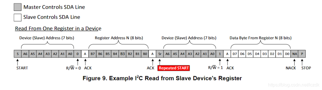
3.2 Reading from a Slave on the I2C Bus

Reading data from a slave is similar to writing data, but with some additional steps. To read from a slave, the master must first indicate which register it wants to read from. This is done by executing the same initial communication steps as the write operation, sending the device address with the read/write bit set to 0 (indicating a write operation), followed by the address of the register to be read. Once the slave acknowledges this address, the master will send a START condition again and send the device address with the read/write bit set to 1 (indicating a read operation). The slave will then acknowledge the read request, while the master releases the bus but keeps supplying the clock to the slave. In this part of the communication process, the master will act as the receiving master, while the slave will act as the sending slave.
The master will continue to send clock pulses but will release the SDA line to allow the slave to transmit data. At the end of each byte of data, the master will send an ACK to the slave to let it know that it is ready to receive more data. Once the master has received the expected number of bytes, it will send a NACK to inform the slave to terminate communication and request the slave to release the bus. The master will then send a STOP condition to end communication. Figure 9 shows an example of reading a single byte from the slave register.
Understanding the I2C Bus
This is a Chinese translation of the Texas Instruments application document SLVA704, originally titled: Understanding the I2C Bus. Compared to the dozens of pages of the I2C standard document published by Philips, this document is only 8 pages long, but it is sufficient for those who want to understand and apply the standard I2C bus.

Original
Source
At:

Original document address: https://www.ti.com/lit/an/slva704/slva704.pdf

Copyright belongs to the original author
or
Platform
All
for learning
reference and academic research
If there is infringement, please contact
to delete ~ thank you

END
Evaluation Center Free Application

Understanding the I2C Bus

Understanding the I2C Bus

👆 Long press the image, scan the code to apply 👆

Leave a Comment