Microcontroller Basics and Applications: Serial Expansion

Click the blue text to follow us

Microcontroller Basics and Applications: Serial Expansion

1. Overview of Microcontroller Serial Expansion

The methods for implementing microcontroller serial expansion include commonly used serial bus standards such as: I2C bus, Serial Peripheral Interface (SPI), and Universal Serial Bus (USB). This chapter will focus on the I2C bus.

1. Implementation through dedicated serial standard bus

(1) Serial Peripheral Interface (SPI)

SPI (Serial Peripheral Interface) is a synchronous serial interface standard with a 3-wire structure, requiring only 4 lines to interface with various standard peripheral devices. It uses full-duplex 3-wire synchronous data transmission and supports a multi-master/slave structure.

(2) Universal Serial Bus (USB)

The USB (Universal Serial Bus) standard was primarily developed by Intel, in collaboration with several world-renowned computer and communication companies. Its characteristics include:

① Simple wiring and ease of use.

② Transmission rates range from a few kbps to several Mbps, suitable for medium to low-speed device interfaces.

③ Strong error correction capabilities, resulting in high reliability.

(3) Access Bus

The ACCESS bus was developed by DEC and is a bidirectional bus that can connect up to 125 external devices. All external devices that support this bus have a port connector similar to a telephone plug and are connected in a daisy chain manner.

2. Implementation through serial communication port UART

Using the UART working mode 0 of the 80C51 microcontroller enables the serial I/O interface function for data transmission between the microcontroller and external devices or control devices.

3. Implementation through software simulation

Software simulation methods can also be used to implement serial interfaces via parallel port lines. However, the interface functionality will be limited, so this method is only suitable for the simplest serial interface applications.

2. I2C Bus

I2C (Inter Integrated Circuit) bus is a serial synchronous communication technology developed by Philips for the needs of microcontrollers, used to achieve serial peripheral expansion of microcontrollers. The I2C bus enables serial data transmission through the coordination of two lines and two sets of signals.

1. Structure and Signal of I2C Bus

The I2C bus has strict specifications that are reflected in aspects such as electrical performance of the interface, signal timing, signal transmission definitions, bus state settings and handling, as well as bus management rules.

(1) Structure of I2C Bus

The I2C bus consists of a serial clock line SCL (Serial Clock Line) and a serial data line SDA (Serial Data Line), forming a bidirectional data transmission path, where SCL transmits the clock signal and SDA transmits the data signal. In a microcontroller serial system formed by the I2C bus, the microcontroller and various peripheral chips and devices connected to the bus are collectively referred to as devices, as shown in the figure below.
An I2C bus system allows multiple devices to be connected, and different transmission rates are permissible, even allowing for another remote I2C system’s driving circuit, thus forming interconnections between two I2C systems.
(2) Device Connection to I2C Bus
Both lines of the I2C bus, SCL and SDA, are connected to the I2C bus through pull-up resistors (typically 10 kΩ) in an open-drain or open-collector output form.
The connection of devices to the I2C bus results in the following hardware relationship: Each device in the bus system has a logical “AND” relationship with the SCL line and also a logical “AND” relationship with the SDA line. Conversely, for low levels, there is a logical “OR” relationship, meaning that any device outputting a low level will pull the connected bus low. This relationship gives the I2C bus a significant advantage: devices can be connected or disconnected at any time without adversely affecting the system. Additionally, it can be seen from the figure that both SCL and SDA are bidirectional transmission lines, as each device contains both input and output controls.

(3) Status and Signals of I2C Bus

1) Bus Idle

Both SCL and SDA are in a high state, indicating that the bus is idle.

2) Bus Occupation and Release

If a device wants to use the bus, it must first occupy it. The master device occupying the bus sends clock signals on the SCL line. After data transmission is completed, the bus should be released promptly, restoring it to an idle state.

3) Clock Signal and Data Signal

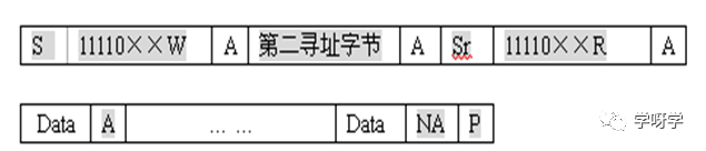
Clock signals appear on the SCL line, while data signals are transmitted on the SDA line. Data is transmitted bit by bit, with one clock cycle transmitting one bit of data. A high level on the SDA line represents data bit 1, while a low level represents data bit 0. The relationship between the clock signal and data signal is: during the high level of the clock signal, the state of the data line must remain stable; only when the clock signal is low can the state of the data bit change. As shown in the figure below.

4) Start and Stop Signals

Start and stop signals can only be issued by the master device, corresponding to the high level of SCL and the transition on SDA. When the SCL line is high, the master device generates a negative level transition on the SDA line, indicating a start signal. When the SCL line is high, the master device generates a positive level transition on the SDA line, indicating a stop signal. After the stop signal appears, a certain time interval must be allowed before the bus can be considered released and return to an idle state.

Typically, the start signal is denoted by S, and the stop signal is denoted by P.

Additionally, during data transmission, a start signal may also occur, but this start signal is referred to as a repeated start signal, denoted by Sr, issued to initiate a new data transmission that differs from the previous one.

5) Acknowledge and Non-Acknowledge Signals

The acknowledge signal confirms the transmission of a byte of data, and after each byte of data transmission is completed, the receiving device should return an acknowledge signal.

The acknowledge signal and non-acknowledge signal correspond to the 9th clock pulse, where the SDA line remains high for a non-acknowledge signal. In practice, the acknowledge signal is represented by ACK (or A), while the non-acknowledge signal is represented by NACK (or NA).

6) Wait State

  • In the I2C bus, the receiving device is granted the authority to put the system into a wait state, but this wait state can only occur after a complete data byte has been received.
  • In the wait state, the sender cannot send data until the receiving device determines that it can continue receiving data, at which point it releases the SCL line, allowing the system to exit the wait state, and the sender can then continue sending data.
  • The wait state is also known as the delay state, essentially changing the data transmission rate by extending the clock pulse cycle. The purpose of setting a wait state is twofold: to provide the receiving device with an opportunity to perform other operations, and to allow the system to connect devices with different speeds. Therefore, the I2C bus system does not impose speed requirements on connected devices.

2. Data Transmission Methods of I2C Bus

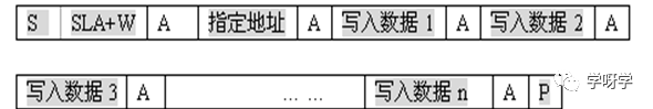
(1) Basic Data Transmission Format

Data transmission on the I2C bus occurs bit by bit, with the high bit first and the low bit second. Each time a data byte is transmitted, an acknowledge signal is used to confirm, and there is no limit to the number of bytes transmitted. The transmission format is shown in the figure below.

(2) Master Transmit Mode

Master transmit mode refers to the master device sending data to the controlled slave device. The data transmission format in master transmit mode is shown in the figure below.

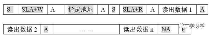
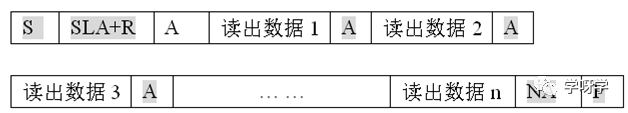
(3) Master Receive Mode

The master device receives data sent from the controlled slave device, which is referred to as master receive mode. Its data transmission format is shown in the figure below.

3. Device Addressing

(1) Device Classification

According to control relationships, there is a control and controlled relationship (or master-slave relationship) between devices. The controlling device is called the master device, while the controlled device is referred to as the slave device.

According to the data transmission relationship, there is a sending and receiving relationship between devices, where the device sending data is called the sender, and the device receiving data is called the receiver.

(2) Device Working Modes

Devices in the bus system have four working modes: master transmit mode (the device sends data as the master), master receive mode (the device receives data as the master), slave transmit mode (the device sends data as the slave), and slave receive mode (the device receives data as the slave).

(3) In the I2C bus system, since there are no address lines available, addresses can only be transmitted via the serial line SDA. Users are concerned with device addressing, specifically how to locate the slave device.

1) Device Addressing

In the I2C bus, device addressing is also known as the slave address. After the I2C bus starts, the first byte sent by the master device is the addressing byte, denoted as SLA+R/W, where the first 7 bits of SLA represent the slave address. The I2C device addressing is uniformly allocated by the I2C bus committee and follows certain rules.

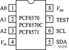
For example: PCF8574 (I2C bus to 8-bit parallel bus converter)
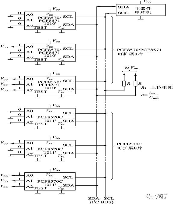
2) Pin Address

The bits A2A1A0, A1A0, and A0 in the addressing bits indicate that their corresponding bits’ encoding is obtained through external levels. These bits of device encoding are set through pins, hence referred to as pin addresses. The pin addresses of the chip are always arranged starting from the lowest bit.

3. I2C Bus of Microcontroller 8×C552

1. I2C Bus Interface Circuit of 8×C552
(1) Structure of I2C Bus Interface
The microcontroller chip 8×C552 retains the original UART serial communication port while adding an I2C bus interface. The original serial port used for serial communication is called SIO0, while the I2C bus interface is named SIO1. The circuit structure of SIO1 is shown in the figure below.
The basic logic of the I2C bus interface consists of bus input/output circuits, comparators, serial clock generators, bus contention and synchronization logic, as well as timing and control logic.
① Bus Input/Output Circuit. Both SCL and SDA are bidirectional lines. The bidirectionality of SCL is due to the master device needing to send clock signals through it while also monitoring its level changes to determine the signal changes on the SDA line.
② Comparator. The comparator is used for address comparison.
③ Bus Contention and Synchronization Logic. The arbitration and clock synchronization of the I2C bus contention rely entirely on hardware circuits, requiring no manual intervention.
④ Serial Clock Generator. The SCL clock pulse is provided by the master device; therefore, the 8×C552 has a programmable serial clock generator to issue clock pulses to the bus when it acts as the master device. When the 8×C552 acts as a controlled slave device, the clock generator is disabled. The frequency of the clock pulse is selected by setting the relevant bits in the control register S1CON in the bus interface circuit.
⑤ Timing and Control Logic. The timing and control logic generates timing and control signals used during serial data transmission, and is also responsible for generating start and stop signals, detecting start and stop signals, and detecting acknowledge signals, among other things. Additionally, the master-slave relationship of data transmission, interrupt requests, and state decoding of the I2C bus are also controlled by the timing control logic.
In the 8×C552 chip, there are no dedicated I2C clock and data signal lines; instead, two lines from port P1 are borrowed: P1.6 — SCL (I2C bus clock signal line); P1.7 — SDA (I2C bus data signal line).
(2) Dedicated Registers for I2C Bus
The I2C bus interface circuit of the 8×C552 also contains four dedicated registers: Address Register S1ADR, Data Register S1DAT, Control Register S1CON, and Status Register S1STA.
The Address Register is an 8-bit read/write register, with the address being 0DBH, used to store the 7-bit device addressing and the broadcast call identification bit GC’s status.
The content of the S1ADR register is written by the user through a program, with the least significant bit GC used to specify whether to respond to a broadcast call: GC=1 for response; GC=0 for no response.
(3) I2C Bus Interrupt
The microcontroller chip 8×C552 with an I2C interface has introduced a new interrupt type, the I2C interrupt, specifically for data transmission on the I2C bus. Whenever a basic operation is completed on the bus, a status code is generated, and the hardware sets the interrupt enable bit ESI in the interrupt enable register IE0. If the interrupt system is open and the I2C interrupt is enabled, an I2C interrupt request is generated.
2. Control Mechanism of I2C Bus in 8×C552
(1) Status Codes of I2C Bus
The so-called status refers to the state of the circuits in the I2C bus interface after the execution of a basic operation subroutine, while status codes are the binary encoding of that state.
In the I2C bus interface circuit of the 8×C552, there are status decoding circuits and status code registers. After each basic operation is completed, the status decoding circuit generates a 5-bit status code. The status code is stored in an 8-bit status code register, occupying its high 5 bits, while the low 3 bits are filled with 0, resulting in an 8-bit status code. Since the low 3 bits are 0, the code values of the status codes differ by 8. The I2C bus has a total of 26 basic operations, resulting in 26 corresponding status codes. The status code table is omitted.
(2) I2C Bus Protocol Driver
The I2C bus employs a data transmission method that utilizes status codes obtained from previous operations and interrupts to guide subsequent operations.
ORG0000H
STRT: LJMPMAIN ; Jump to application program after system reset
ORG002BH
IICI: PUSHPSW ; I2C interrupt service routine
PUSHS1STA
PUSHHADD
RET ; Return to the corresponding subsequent processing subroutine
ORG00A0H
INITS1: MOVPSW,#18H ; Select register group
MOVR1,#MTD ; Send data buffer starting address
MOVR0,#MRD ; Receive data buffer starting address
MOVBACKUP,NUMBYT ; Number of bytes
POPPSW ; Restore program status word
RETI
3. Single Master I2C Bus System Composed of 8×C552
The data transmission in a single master I2C bus system only involves master transmit and master receive modes. Among the 26 status codes of the I2C bus, the data transmission and reception operations in the single master mode only involve 10 codes: 08H, 10H, 18H, 20H, 28H, 30H, 40H, 48H, 50H, and 58H.
(1) Example Application of Single Master System
Assuming the master device is the microcontroller 8×C552 and the controlled slave device is a memory chip, only the master transmit mode can be used.
Transmission Program Design
MAIN: MTD EQU 30H
MRD EQU 38H
SRD EQU 40H
STD EQU 48H
HAAD EQU 50H
SLA EQU 51H
NUMBYT EQU 52H
BACKUP EQU 53H
MOVS1ADR, #××H ; Write the device address of 8×C552
SETBP1.6 ; Set port line latch to 1 for I2C bus usage
SETBP1.7
MOVHAAD, #01H ; Set the high 8 bits of the program address
ORLIE0, #0A0H ; Enable I2C bus interrupt system
CLR0BDH ; Set to low priority
MOVS1CON, #0C5H ; Enable I2C bus interface, set clock frequency
MOVNUMBYT, #08H ; Number of data bytes to transmit
MOVSLA, #0A0H ; Address byte SLA+W
SETBSTA ; Start I2C bus operation
Note: When in use, the system will jump to the bus driver program immediately after reset, and after executing the first jump instruction LJMP, it will proceed to this transmission program MAIN. The operation flow of the single master system is shown in the figure below.
Interrupt Handling Program
The interrupt handling program is located in the bus driver program, named IICI.
IICI: PUSHPSW
PUSHS1STA
PUSHHADD
RET
Note: During program execution, the stack data order is: breakpoint address, PSW, S1STA, and HADD. When executing the RET instruction, following the “last in, first out” rule, the order of popping from the stack becomes: HADD, S1STA, PSW, and breakpoint address. As a result, the content of HADD and S1STA is sent as a breakpoint to the PC, allowing the program to return to the corresponding subsequent operation subroutine according to the current status code.
(2) Description of Data Transmission Process
1) SI08 (Start signal is normally issued, preparing to send SLA+R/w and receive acknowledge signal)
After completing the interrupt handling, PC=0108H, it proceeds to execute the SI08 operation subroutine. In the SI08 program, the first step is to write SLA+W into the interface data register and send it out, followed by setting the clock frequency and preparing to receive the acknowledge signal. Then it calls the lower-level subroutine INITS1.
2) SI18 (After issuing SLA+W, receive acknowledge signal, preparing to send the first data byte)
After executing the interrupt program, it goes to the SI18 state operation subroutine. In the SI18 subroutine, it also first selects the register group, then sends the data to the data register S1DAT, and then jumps to the lower-level subroutine CON.
3) SI28 (After sending a data byte and receiving an acknowledge signal, preparing to continue sending data bytes or stop signal)
In the SI28 subroutine, the byte count is decremented by 1, and if the result is not 0, it goes to the lower-level subroutine NOLD1. The next data is sent through NOLD1. The status code received after the acknowledge signal is still 28H, allowing for repeated data transmission.

4. Serial Expansion of Microcontroller 8×C552

1. Serial Data Memory Expansion via I2C Bus
(1) Overview of PCF8571/8570/8570C Chips
PCF8571/8570/8570C are low-power CMOS static RAM chips with I2C bus interfaces. The PCF8571 has a capacity of 128 bytes, with a device code of 1010; the PCF8570 has 256 bytes, also with a device code of 1010; and the PCF8570C has 256 bytes, with a device code of 1011. The pin diagram is as follows:

Microcontroller Basics and Applications: Serial Expansion

In the I2C bus system, the PCF8571/8570/8570C chips can only act as controlled slave devices, hence their hardware structure is relatively simple, with only 8 pins: A2, A1, A0 for address pins, SDA for data line, SCL for clock line, TEST for test pin (ground when not used), VDD for positive power supply, and VSS for negative power supply (ground).
(2) Data Read/Write Operations
The PCF8571/8570/8570C memory chips have only three data operation forms: specified address write, specified address read, and current address read.
  • Specified Address Write

Microcontroller Basics and Applications: Serial Expansion

  • Specified Address Read

Microcontroller Basics and Applications: Serial Expansion

  • Current Address Read

Microcontroller Basics and Applications: Serial Expansion

(3) Serial Data Memory Expansion Connection Since the capacity of the PCF8571/8570/8570C memory chips is relatively small, when the external storage capacity is large, it is often necessary to connect multiple chips. The figure below shows a multi-chip data storage expansion system.
Although both PCF8570 and PCF8570C are memory chips, due to their different high 4-bit device addressing, they are considered different types of devices, allowing them to be connected simultaneously in a single bus system. That is, in an I2C bus system, up to 8 pieces of PCF8571/8570 and 8 pieces of PCF8570C can be expanded simultaneously, totaling 16 RAM chips.

Microcontroller Basics and Applications: Serial Expansion

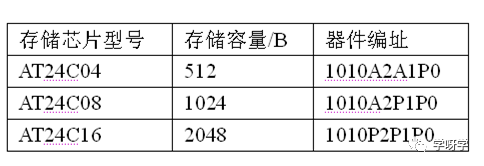
Multi-chip data storage expansion in I2C bus system

2. Development of I2C Bus
Expanding the system, increasing the number of devices, and enhancing storage capacity are important aspects of I2C bus development.
(1) Page Addressing
The figure illustrates three chips with page addresses.

Microcontroller Basics and Applications: Serial Expansion

The AT24C04 chip uses P0 as the page address, where a 1-bit page address can represent 2 pages; when P0=0, it points to the lower 256 units, and when P0=1, it points to the upper 256 units. The AT24C08 and AT24C16 chips have 2-bit and 3-bit page addresses, respectively, allowing them to represent 4 pages and 8 pages.
(2) 10-bit Addressing Mode
The so-called 10-bit addressing mode refers to increasing the device addressing from 7 bits to 10 bits. The 10-bit addressing mode is a trend in the development of the I2C bus, aimed at increasing the number of devices in the system.
1) Addressing Process in 10-bit Addressing Mode
To maintain compatibility with the 7-bit addressing mode, the addressing increment must be conducted without altering the original I2C bus protocol. The addressing byte is increased from one to two, requiring two transmissions. These two bytes are referred to as the first addressing byte and the second addressing byte, respectively.
The content of the first addressing byte is fixed as 11110××W, where the high 5 bits 11110 serve as the flag for the 10-bit addressing mode, “××” represents the highest 2 bits in the 10-bit device addressing, and W indicates the direction bit (write). Following this, the second addressing byte is sent, using the 2 bits “××” from the first addressing byte as the high bits and the entire second addressing byte as the low 8 bits, forming a 10-bit addressing address.
2) Data Transmission Format in 10-bit Addressing Mode
n master device sends data

Microcontroller Basics and Applications: Serial Expansion

n master device receives data

Microcontroller Basics and Applications: Serial Expansion

3. Expansion of LED Display via I2C Bus
(1) LED Driver Chip SAA1064
SAA1064 is a typical dedicated LED driver chip in the I2C bus system, with a device code of 0111, featuring two sets of 8-bit segment code driver outputs, packaged in a 24-pin dual in-line package, as shown in the figure below.
Microcontroller Basics and Applications: Serial Expansion
(2) Interface Connection and Operation of SAA1064

Microcontroller Basics and Applications: Serial Expansion

SAA1064 static display mode interface connection

Microcontroller Basics and Applications: Serial Expansion

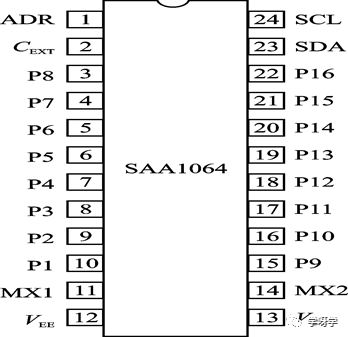
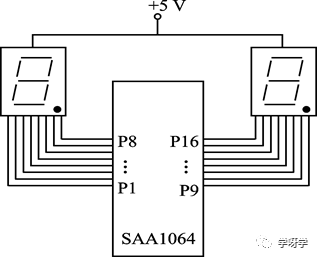
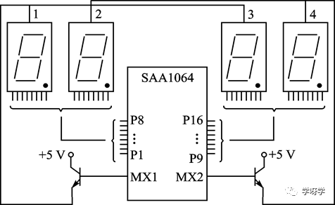
SAA1064 dynamic display mode interface connection

(3) Features of SAA1064
Compared to parallel LED display interfaces, SAA1064 can not only drive LED displays but also possesses some control functions. The control functions are defined by the control word, with the bit format represented as follows:

Microcontroller Basics and Applications: Serial Expansion

D7——Unused;
D6, D5, D4——Display brightness control, D6D5D4=111 for maximum brightness;
D3——Test bit, D3=1 turns on all segments of the LED;
D2——Display 2, 4 bit brightness selection bit, D2=1 for on;
D1——Display 1, 3 bit brightness selection bit, D1=1 for on;
D0——Display mode selection bit, D0=1 for dynamic mode, D0=0 for static mode. Thus, the control functions of SAA1064 include: selecting display mode, bit-wise selection for on/off, and adjusting the LED display brightness (achieved by changing the driving current).
Unlike other I2C bus devices, SAA1064 has an analog address pin ADR, which corresponds to four pin addresses based on the size of the connected analog voltage, specifically A1A0=00, A1A0=01, A1A0=10, and A1A0=11. As a result, one ADR pin serves the same function as two address pins A1 and A0, thereby reducing the number of pins. Because it can form four pin addresses, a maximum of four SAA1064 chips can be connected in an I2C bus system.

5. Serial Expansion of Microcontroller 80C51

1. Serial Program Memory Expansion via UART

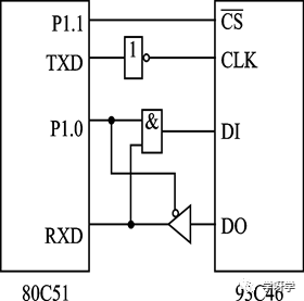
Serial program memory expansion typically uses serial EEPROM chips for electrically erasable programmable read-only memory. In such chips, some can be expanded via UART, such as the 93C46. The pin arrangement of this chip is shown in the figure below.

Connecting the serial memory expansion via the UART of the 80C51 is not complicated; for example, the connection of the 93C46 is shown in the figure below.

Microcontroller Basics and Applications: Serial Expansion

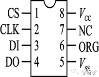
93C46 Chip Pin Arrangement

Microcontroller Basics and Applications: Serial Expansion

Connection of Serial Memory Expansion via UART

2. Software Simulation of Serial Interfaces

Serial interface functions can also be achieved through software simulation, i.e., using software-driven serial data transmission on parallel port lines, which is commonly used in simple systems without serial interfaces. Taking the serial interface of the 80C51 and PCF8582 as an example, we will illustrate the software simulation method for the I2C bus interface.

Using P3.4 and P3.5 of the 80C51 as the serial clock line SCL and serial data line SDA, the circuit connection is shown in the figure below.

Microcontroller Basics and Applications: Serial Expansion

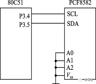
In the 80C51 chip, since there are pull-up resistors within port P3, external pull-up resistors are not required. On the PCF8582 chip, A2, A1, A0 are grounded, which means the pin address is 000.

To start the I2C bus, both the SCL and SDA lines should be set high, and after a delay, the SDA line should be pulled low. The following sequences of instructions call or jump to the delay subroutine DELAY, which is merely to indicate that a time delay is required at that point.

SCL EQU 0B4H

SDA EQU 0B5H

SETB SCL

NOP

NOP

SETB SDA

ACALLDELAY

CLR SDA

PCF8582 has an I2C bus interface circuit that can detect the start signal on the bus and subsequently enter working state to receive the addressing byte sent by the 80C51.

In the I2C bus, data transmission occurs with the high bit first and the low bit second, hence the loop left shift instruction RLC is used to shift the data into the carry flag C first, followed by the bit transfer instruction to send it out. The two instructions are as follows:

RLC A

MOV SDA,C

After PCF8582 receives a byte of data, it should return an acknowledge signal. To receive the acknowledge signal from PCF8582, the simulation program of the 80C51 should release the SDA line to make it high. Additionally, the SCL line should be set high and then low to generate the 9th clock pulse. The sequence of instructions is as follows:

SETB SDA

ACALL DELAY

SETB SCL

ACALL DELAY

CLR SCL

If the operation is to read from PCF8582, after the 80C51 receives a byte of data, it sends an acknowledge signal to PCF8582 by pulling SDA low and generating the 9th clock pulse. The instruction sequence for this is as follows:

CLR SDA

ACALL DELAY

SETB SCL

ACALL DELAY

CLR SCL

The stop signal should be issued by the 80C51, as shown in the instruction sequence below:

CLR SDA

NOP

NOP

SETB SCL

ACALL DELAY

SETB SDA

3. I2C Bus Interface Chip PCF8584

For microcontrollers like the 80C51 that lack an I2C bus interface, the I2C bus interface chip can be utilized to perform I2C bus operations. A typical I2C bus interface chip is the PCF8584, which primarily functions to convert from parallel bus to I2C bus.

(1) Logical Structure of PCF8584

Microcontrollers interfacing with PCF8584 can act as master devices in the I2C bus system, so the hardware structure of the PCF8584 chip is relatively complex. Its logical structure is shown in the figure below.

Microcontroller Basics and Applications: Serial Expansion

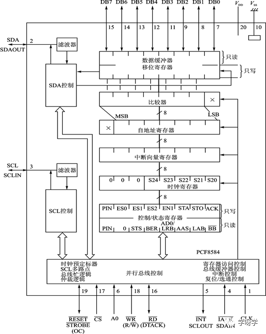
The conversion between parallel bus and I2C bus is achieved through a data register. The data register is a combination of a data buffer and a shift register, connecting to the parallel bus through the data buffer and to the I2C bus through the shift register. Both share a common address, thus referred to as the data register.

When the PCF8584 interface chip needs to send data to the I2C bus, the parallel data is directly written into the serial shift register, then shifted onto the SDA line. When receiving data, serial data is shifted from the SDA line into the shift register, and when the acknowledge signal appears, the data is copied from the shift register to the data buffer, then read into the CPU via the parallel bus.

The control register, status register, and self-address register are introduced below. The control and status registers share a common address and can be referred to as control/status registers.

Microcontroller Basics and Applications: Serial Expansion

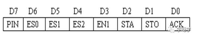
The control register is an 8-bit write-only register, with bit format and main control bit definitions as follows:

PIN——Interrupt control bit; ES2~ES0——Register selection bits;

ENI——Interrupt enable bit; STA——Start signal control bit;

STO——Stop signal control bit; ACK——Acknowledge signal control bit.

Microcontroller Basics and Applications: Serial Expansion

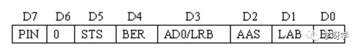
The status register is an 8-bit read-only register, with bit format and main control bit definitions as follows:

PIN——Interrupt control bit; STS——Stop status flag bit;

BER——Bus error flag bit; AD0——Zero address bit;

LRB——Last received flag bit; AAS——Slave device addressing bit;

LAB——Arbitration failure bit; BB——Bus busy flag bit.

The self-address register can also be referred to as the slave address register; it is also an 8-bit register (only using 7 bits) used to store the device code of this chip.

(2) Connecting 80C51 to I2C Bus via PCF8584

The main interface function of PCF8584 is to connect the microcontroller to the I2C bus system. Its connection with the 80C51 is shown in the figure below.

Microcontroller Basics and Applications: Serial Expansion

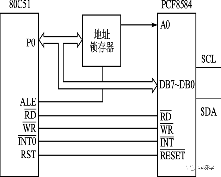
Connection of 80C51 with PCF8584

Microcontroller Basics and Applications: Serial Expansion

Long press the image to follow

Discover more exciting content

WeChat ID: Mechanical-knowledge

Leave a Comment