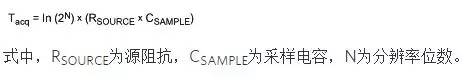
Acquisition time is the time required for the sample-and-hold circuit to stabilize the sample capacitor voltage within 1 LSB range of the new input value after releasing the hold state.The formula for acquisition time (Tacq) is as follows:
According to the sampling theorem, input signal frequencies above the Nyquist frequency are referred to as “aliasing” frequencies.In other words, these frequencies are “folded” or replicated into other spectral positions near the Nyquist frequency.To prevent aliasing, all harmful signals must be sufficiently attenuated so that the ADC does not digitize them.In undersampling, aliasing can be a favorable condition.
The aperture delay (tAD) in an ADC is the time interval from the sampling edge of the clock signal (the rising edge of the clock signal in the figure below) to when the sampling occurs.Sampling is performed when the ADC’s track-and-hold switches to the hold state.
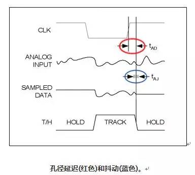
Aperture jitter (tAJ) refers to the variation in aperture delay between samples, as shown in the figure.Typical values of ADC aperture jitter are much smaller than the aperture delay value.
Binary Encoding (Unipolar)
Quasi-binary is a commonly used encoding method for unipolar signals. The range of binary codes (from zero to full scale) is from all 0s (00…000) to all 1s of the positive full-scale value (11…111). The middle value is represented by a 1 (MSB) followed by all 0s (10…000). This encoding is similar to offset binary encoding, which supports both positive and negative bipolar transfer functions.
The term “bipolar” refers to signals oscillating above and below a certain reference level. In a single-ended system, the input is usually referenced to ground, so a bipolar signal is one that oscillates above and below ground level. In a differential system, the signal is not referenced to ground, but rather the positive input is referenced to the negative input; thus, a bipolar signal refers to the positive input signal being able to be higher and lower than the negative input signal.
Common Mode Rejection (CMRR)
Common mode rejection refers to the ability of a device to suppress the common mode signals of two inputs. Common mode signals can be AC or DC signals, or a combination of both. The common mode rejection ratio (CMRR) is the ratio of differential signal gain to common mode signal gain. CMRR is usually expressed in decibels (dB).
Crosstalk refers to the degree of isolation between each analog input and other analog inputs. For ADCs with multiple input channels, crosstalk refers to the total amount of signal that couples from one analog input signal to another, usually expressed in decibels (dB); for DACs with multiple output channels, crosstalk refers to the total amount of noise generated at one DAC output when another DAC output is updated.
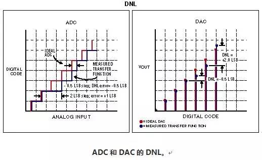
Differential Nonlinearity (DNL) Error
For ADCs, the difference in analog input levels triggering any two consecutive output codes should be 1 LSB (DNL = 0), and the actual level difference relative to 1 LSB deviation is defined as DNL. For DACs, DNL error is the difference between the ideal and measured output responses of consecutive DAC codes. The ideal DAC response’s analog output values should strictly differ by one code (LSB) (DNL = 0). (DNL values greater than or equal to 1 LSB guarantee monotonicity.) (See “Monotonicity.”)
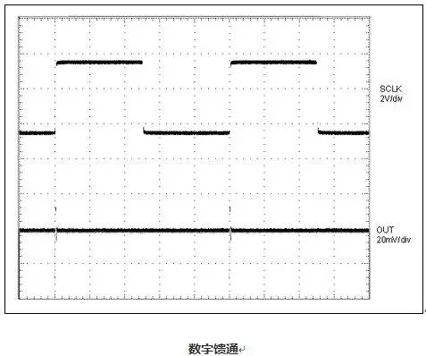
Digital feedthrough refers to the noise generated at the DAC output when the digital control signal changes. In the figure below, the feedthrough at the DAC output results from the serial clock signal noise.
The dynamic range is defined as the range between the device’s background noise and its specified maximum output level, usually expressed in dB. The dynamic range of an ADC is the range of signal amplitudes that the ADC can resolve; if the dynamic range of the ADC is 60 dB, then the resolvable signal amplitudes are from x to 1000x. In communication applications, the range of signal strength varies significantly, making dynamic range very important. If the signal is too large, it will cause the ADC input to exceed range; if the signal is too small, it will be drowned in the converter’s quantization noise.
Effective Number of Bits (ENOB)
ENOB represents the dynamic performance of an ADC at a specific input frequency and sampling rate.The error of an ideal ADC only includes quantization noise.As the input frequency increases, the overall noise (especially the distortion component) also increases, thereby reducing ENOB and SINAD (see “Signal to Noise and Distortion Ratio (SINAD)”).The ENOB for full-scale, sinusoidal input waveforms is calculated as follows:
A measurement technique where voltage (or current) is loaded at the far end of the circuit, and then the resulting current (or voltage) is measured (detected). For example, a DAC with an integrated output amplifier sometimes includes load-induced output. The output amplifier can provide an inverting input for external connection, and the feedback path must be formed externally to close the loop.
Full-Power Bandwidth (FPBW)
The analog input signal applied during ADC operation equals or approaches the converter’s specified full-scale voltage. The input frequency is then increased to a frequency that reduces the magnitude of the digital conversion result by 3 dB. This input frequency is the full-power bandwidth.
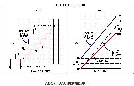
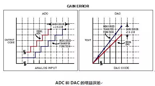
Full-scale error is the difference between the actual value that triggers a transition to full-scale code and the ideal analog full-scale transition value. Full-scale error equals “offset error + gain error,” as shown in the figure below.
The full-scale gain error of a Digital to Analog Converter (DAC) is the difference between the actual and ideal output span. The actual span is the difference between the output when the input is set to all 1s and when the input is set to all 0s. The full-scale gain error of all data converters is related to the reference used to measure the gain error.
The gain error of an ADC or DAC indicates the degree of match between the slope of the actual transfer function and the slope of the ideal transfer function.Gain error is usually expressed as a percentage of LSB or full-scale range (%FSR) and can be eliminated through hardware or software calibration.Gain error equals full-scale error minus offset error.
Gain error drift refers to the change in gain error caused by environmental temperature, usually expressed as ppm/°C.
Gain consistency indicates the degree of match of gains across all channels in a multi-channel ADC.To calculate gain consistency, the same input signal is applied to all channels, and the maximum gain deviation is recorded, usually expressed in dB.
A spike pulse refers to the transient voltage oscillation generated at the DAC output when the MSB transitions, usually expressed as nV?s, equal to the area under the voltage-time curve.
The harmonics of a periodic signal are the sine components that are integer multiples of the signal’s fundamental frequency.
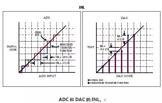
Integral Nonlinearity (INL) Error
For data converters, integral nonlinearity (INL) is the deviation of the actual transfer function from the linear transfer function. After eliminating offset error and gain error, this linear function is the best-fit line or the line between the endpoints of the transfer function. INL is often referred to as “relative accuracy.”
Intermodulation Distortion (IMD)
IMD refers to the phenomenon of new frequency components that do not exist in the original signal due to the nonlinearity of the circuit or device. IMD includes harmonic distortion and two-tone distortion. During measurement, it is expressed as the total power of the selected intermodulation products (i.e., IM2 to IM5) relative to the total power of the two input signals (f1 and f2). The 2nd to 5th order intermodulation products are as follows:
·2nd Order Intermodulation Product (IM2): f1 + f2, f2 – f1
·3rd Order Intermodulation Product (IM3): 2 x f1 – f2, 2 x f2 – f1, 2 x f1 + f2, 2 x f2 + f1
·4th Order Intermodulation Product (IM4): 3 x f1 – f2, 3 x f2 – f1, 3 x f1 + f2, 3 x f2 + f1
·5th Order Intermodulation Product (IM5): 3 x f1 – 2 x f2, 3 x f2 – 2 x f1, 3 x f1 + 2 x f2, 3 x f2 + 2 x f1
Least Significant Bit (LSB)
In binary numbers, the LSB is the lowest weighted bit.Typically, the LSB is the rightmost bit.For an ADC or DAC, the weight of the LSB equals the full-scale voltage range of the converter divided by 2N, where N is the resolution of the converter.For a 12-bit ADC, if the full-scale voltage is 2.5V, then 1 LSB = (2.5V/2^12) = 610μV
During the MSB transition (mid-scale point), the MSB changes from low to high, while all other data bits change from high to low; or the MSB changes from high to low, while all other data bits change from low to high. For example, 01111111 changing to 10000000 is an MSB transition. MSB transitions often produce the most severe switching noise (see spike pulse).
A sequence is said to be monotonically increasing if, for each n, Pn + 1 is always greater than or equal to Pn; similarly, if for each n, Pn + 1 is always less than or equal to Pn, the sequence is said to be monotonically decreasing.For a DAC, if the analog output always increases with an increase in DAC code input, then the DAC is said to be monotonic; for an ADC, if the digital output code always increases with an increase in analog input, then the ADC is said to be monotonic.If the DNL error of the converter does not exceed ±1 LSB, monotonicity can be guaranteed.
Most Significant Bit (MSB)
In binary numbers, the MSB is the highest weighted bit. Typically, the MSB is the leftmost bit.
Multiplying DACs allow AC signals to be applied to the reference input. By connecting the signal of interest to the reference input and using DAC encoding to scale the signal, the DAC can act as a digital attenuator.
When a rising signal is applied to the analog input of the ADC, if the ADC produces all possible digital encodings, then that ADC is said to have no-loss encoding.
The Nyquist theorem states that the sampling rate of the ADC must be at least twice the maximum bandwidth of the signal to reconstruct the analog signal without distortion. This maximum bandwidth is referred to as the Nyquist frequency.
Offset binary is a commonly used encoding method for bipolar signals. In offset binary encoding, the negative maximum value (negative full-scale value) is represented by all 0s (00…000), and the positive maximum value (positive full-scale value) is represented by all 1s (11…111). Zero amplitude is represented by a 1 (MSB) followed by all 0s (10…000). This method is similar to standard binary, which is often used for unipolar signals (see binary encoding, unipolar).
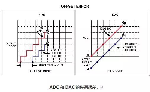
The measurement of offset error in bipolar converters is similar to that in unipolar converters, but measures the error at the zero amplitude point of the bipolar transfer function.
Offset error, often referred to as “zero amplitude” error, refers to the difference between the actual transfer function and the ideal transfer function at a certain operating point. For an ideal data converter, the first transition occurs at 0.5 LSB above zero. For an ADC, the zero amplitude voltage is applied to the analog input and increased until the first transition occurs; for a DAC, the offset error is the analog output when the input code is all 0s.
Offset error drift refers to the change in offset error caused by environmental temperature, usually expressed as ppm/°C.
For ADCs, if the sampling frequency of the analog input is much higher than the Nyquist frequency, it is referred to as oversampling. Oversampling effectively reduces the noise floor, thus improving the dynamic range of the ADC. Increasing the dynamic range further improves the resolution. Oversampling is the basis for Σ-Δ ADCs.
Phase matching indicates the degree of phase matching of the identical signal applied to all channels of a multi-channel ADC. Phase matching refers to the maximum phase shift among all channels, usually expressed in degrees.
Power Supply Rejection Ratio (PSRR)
The power supply rejection ratio (PSRR) is the ratio of the change in power supply voltage to the change in full-scale error, expressed in dB.
For ADCs, quantization error is defined as the difference between the actual analog input and the digital encoding that represents that value (see “Quantization”).
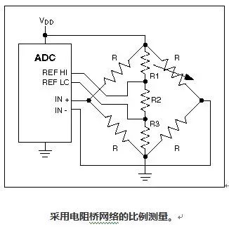
In proportional measurement, the voltage applied to the ADC reference input is not a constant voltage but is proportional to the signal applied to the transmitter (i.e., load cell or bridge). This type of measurement eliminates all errors caused by changes in the reference voltage. The method using a resistor bridge in the figure below is an example of proportional measurement.
The resolution of an ADC is the number of bits used to represent the analog input signal. To reproduce the analog signal more accurately, the resolution must be increased. Using an ADC with higher resolution also reduces quantization error. For DACs, the resolution is similar: the higher the resolution of the DAC, the smaller the step size generated at the analog output when increasing the code.
The RMS value of an AC waveform is the effective DC value or the equivalent DC signal of that signal. To calculate the RMS value of an AC waveform, the AC waveform is first squared and time-averaged, then its square root is taken. For a sine wave, the RMS value is 2/2 (or 0.707) times the peak value, which is 0.354 times the peak-to-peak value.
The sampling rate or sampling frequency is expressed in “samples per second” (sps), indicating the rate at which the ADC samples the analog input. For ADCs that perform one sample per conversion (such as SAR, Flash ADC, or pipeline ADC), the sampling rate also refers to throughput. For Σ-Δ ADCs, the sampling rate is generally much higher than the data output frequency.
For DACs, setup time is the time interval from the command to update (change) its output value to when the output reaches its final value (within a specified percentage). Setup time is influenced by the slew rate of the output amplifier and the total amount of amplifier ringing and signal overshoot. For ADCs, the time required for the sample capacitor voltage to stabilize to 1 LSB is critical to the converter’s capture time.
Signal to Noise and Distortion Ratio (SINAD)
SINAD is the ratio of the RMS value of a sine wave (the input to the ADC, or the output restored by the DAC) to the RMS value of the converter noise plus distortion (non-sine wave). RMS noise plus distortion includes all spectral components below the Nyquist frequency except for the fundamental and DC offset. SINAD is usually expressed in dB.
Signal to Noise Ratio (SNR)
The signal-to-noise ratio (SNR) is the ratio of the useful signal amplitude to the noise amplitude at a given point in time; the higher this value, the better. For waveforms perfectly reconstructed from digital samples, the theoretical maximum SNR is the ratio of the full-scale analog input (RMS value) to the RMS quantization error (residual error). Ideally, the theoretical minimum ADC noise only contains quantization error and is directly determined by the ADC’s resolution (N bits):
(In addition to quantization noise, actual ADCs also produce thermal noise, reference noise, clock jitter, etc.)
In signed binary encoding, the MSB represents the sign (positive or negative) of the binary number. Therefore, the 8-bit representation of -2 is 10000010, and the representation of +2 is 00000010.
The slew rate is the maximum rate of change of the DAC output, or the maximum rate of change of the input that will not cause an error in the ADC digital output. For DACs with output amplifiers, the specified slew rate is usually that of the amplifier.
Small Signal Bandwidth (SSBW)
To measure small signal bandwidth, an analog input signal of sufficiently small amplitude is applied to the ADC, such that the slew rate does not limit the performance of the ADC. The input frequency is then scanned until the magnitude of the digital conversion result decreases by 3 dB. Small signal bandwidth is often limited by the performance of the associated sample-and-hold amplifier.
Spurious-Free Dynamic Range (SFDR)
Spurious-free dynamic range (SFDR) is the ratio of the RMS magnitude of the fundamental (maximum value of the signal component) to the RMS value of the second largest spurious component (excluding DC offset). SFDR is expressed in decibels (dBc) relative to the carrier.
Total Harmonic Distortion (THD)
THD measures the distortion components of a signal, expressed in decibels (dB) relative to the fundamental. For ADCs, total harmonic distortion (THD) is the ratio of the RMS sum of the harmonics of the selected input signal to the fundamental. During measurement, only harmonics within the Nyquist limit are included.
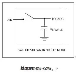
Track-and-hold is often referred to as “sample-and-hold,” referring to the input sampling circuit of the ADC. The most basic representation of track-and-hold input is an analog switch and capacitor (see figure). When the switch is closed, the circuit is in “track” mode; when the switch is open, the sample capacitor holds the last transient value of the input, and the circuit is in “hold” mode.
Conversion noise refers to the range of input voltage changes that cause the ADC output to switch between adjacent output codes.When the analog input voltage is increased, the voltage that triggers each code to transition (code edge) is uncertain due to the associated transient noise.
Two’s Complement Encoding
The two’s complement encoding method is used for encoding both positive and negative numbers, simplifying addition and subtraction calculations. In this encoding method, the 8-bit representation of -2 is 11111110, and the representation of +2 is 00000010.
In undersampling techniques, the ADC sampling rate is lower than the analog input frequency, which can cause aliasing.According to the Nyquist theorem, it is known that undersampling will lose signal information.However, if the input signal is properly filtered and the analog input and sampling frequencies are correctly chosen, the aliased components containing signal information can be shifted from higher frequencies to lower frequencies and then converted.This method effectively uses the ADC as a downconverter, shifting higher bandwidth signals to the effective bandwidth of the ADC.For this technique to succeed, the bandwidth of the ADC track-and-hold circuit must be able to handle the expected highest frequency signal.
For single-ended analog input ADCs, the unipolar signal input range is from zero amplitude (usually ground) to full scale (usually reference voltage); for differential input ADCs, the signal input range is from zero amplitude to full scale, with the positive input corresponding to the negative input measurement range.
See offset error (unipolar).

This account maintains neutrality regarding all original and reprinted articles’ statements and views; the articles pushed are for readers’ learning and communication purposes only. Copyright for articles, images, etc. belongs to the original authors.
For submissions/recruitment/promotion/advertising, please add WeChat: 15989459034