Introduction: A Manufacturing Revolution from “Millimeter” to “Micrometer” Scale
As Moore’s Law approaches its physical limits, the main battleground for increasing chip integration has shifted from wafer processing to advanced packaging. The rise of System-in-Package (SiP), 3D stacking, and heterogeneous integration technologies presents unprecedented challenges for micrometer-level interconnection processes. Traditional stencil printing is limited by minimum aperture sizes (usually >50μm), insufficient demolding accuracy (bridge rate >10%), and poor adaptability to non-planar substrates, making it unable to meet high-density interconnection demands. Microdot solder paste technology, through the synergistic innovation of dynamic driving algorithms and nanomaterials, compresses solder joint diameters to below 80μm, achieving mass production stability with CPK>1.67, effectively breaking the design ceiling for electronic products. This article will deeply analyze how this technology reconstructs manufacturing paradigms from four dimensions: technical principles, core breakthroughs, application scenarios, and future trends.

1. Technical Bottlenecks: The Physical Limits and Design Constraints of Traditional Processes
1.1 The Physical Boundaries of Stencil Printing
Minimum Aperture Limitations: Stencil printing must ensure the matching relationship between solder powder particle size and aperture size (particle diameter ≤ aperture width of 1/5), T6 grade solder powder (3-8μm) requires a 55μm aperture, but bridging can easily occur during demolding (defect rate >5%).
Poor Adaptability to Non-Planar Substrates: For 3D-MID (three-dimensional molded interconnect devices) or flexible substrates, traditional printing leads to solder paste distribution deviation (deviation >20μm) due to uneven stencil contact pressure.
1.2 The Game of Process Cost and Reliability
The Economic Dilemma of Silver Adhesive Die Attach: High silver content (>80%) die attach adhesive costs account for 15% of the total packaging cost, while solder die attach (such as SnSb10Ni0.5 alloy) can reduce costs by more than 50%, while improving thermal conductivity to 45W/m·K.
Void Rate and Thermal Failure: When the void rate of traditional process solder joints exceeds >5%, thermal resistance increases by 30%, while microdot solder technology can suppress the void rate to <2%.
1.3 The Lack of Design Freedom
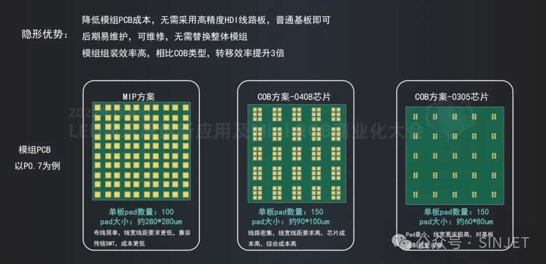
Process Conflicts in Package-on-Package (PoP): Multi-layer chip stacking requires through interconnections, but traditional processes lead to interlayer short-circuit risks due to solder paste volume control deviations (yield <95%). Microdot soldering achieves precise solder application layer by layer (dot diameter 80μm, spacing 35μm), improving yield to 99.9% and effectively avoiding batch soldering defects caused by material expansion and contraction.
2. Technical Breakthroughs: The Trinity of Materials, Equipment, and Algorithms
2.1 Material Innovation: Solder Paste Rheology and Functional Design
Ultra-Fine Powder and Flux Synergy: Heraeus Welco AP520 SAC305 solder paste uses T6SG grade solder powder (particle size 3-8μm), combined with water-soluble flux, achieving 12 hours of continuous printing without bridging defects under a 55μm stencil aperture, with a void rate of <10%.
–Nano-Enhanced and Low-Temperature Compatible: Adding 0.5% nano-silver particles (particle size <50nm) to Sn-Bi low-temperature solder paste, with a melting point of 138℃, reduces thermal resistance by 15%, suitable for Mini LED mass transfer (transfer yield >99.99%).
2.2 Equipment Revolution: From Contact Dispensing to Non-Contact Jetting
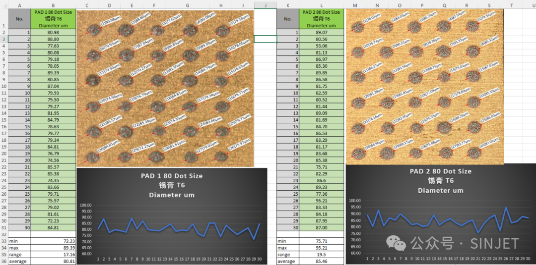
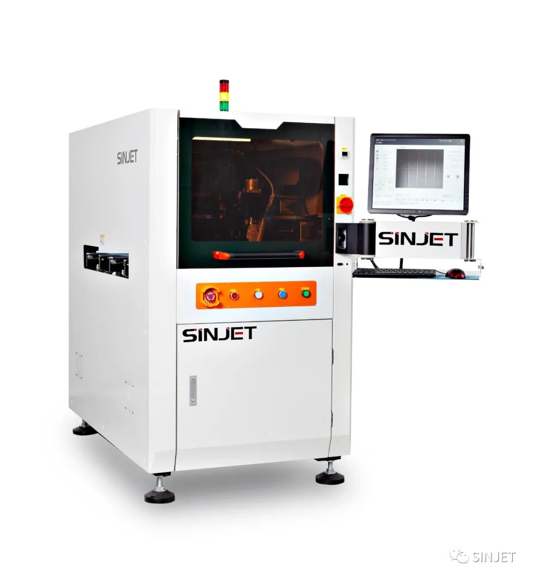
Dynamic Shock Wave Drive Technology (DST): The Shengjie Intelligent Dsniper solder paste valve system uses pulse-driven DST technology, achieving dot diameter accuracy of ±5μm, supporting precise solder application on 80μm pads.
Multi-Axis Coordination and Visual Closed Loop: The Shengjie i350S soldering machine integrates a six-axis motion platform with 3D visual positioning, achieving acceleration of 3G, with a Z-axis repeat positioning accuracy of ±2μm, adapting to dynamic compensation for non-planar substrates.
2.3 Algorithm Empowerment: AI-Driven Process Optimization
Temperature – Pressure Feedback Model: Laser soldering machines monitor solder joint temperatures in real-time through infrared temperature measurement modules (accuracy ±3℃), dynamically adjusting laser power (response time <5ms), avoiding damage to heat-sensitive components.
Defect Prediction and Self-Correction: The deep learning-based SPI (solder paste inspection) system can identify solder paste volume deviations (detection accuracy ±5μm), and adjust jetting parameters through closed-loop control, shortening the process debugging cycle by 30%.
3. Application Scenarios: Penetration Across All Fields from Consumer Electronics to Quantum Devices
3.1 Consumer Electronics: Miniaturization and Flexibility Design
Foldable Screen Smartphone Driver: Using Sn-Bi low-temperature solder paste (melting point 138℃) combined with PI substrates, the bending life is improved from 10,000 times to 100,000 times, with solder joint shear strength exceeding >25N/mm².
–TWS Earphone SiP Module: Integrating Bluetooth, noise reduction, and power management chips within a 4×4mm packaging space, achieving 20μm spacing interconnections through 80μm dot diameter solder paste, compressing module thickness to 1.2mm.
3.2 Automotive Electronics: High Reliability and High-Temperature Requirements
–77GHz Millimeter-Wave Radar: Using SnSb10Ni0.5 high-temperature alloy (melting point 265℃), achieving 0.1mm spacing soldering on FR4 substrates, with temperature rating upgraded to AEC-Q101 Grade 1 (-40℃~150℃).
IGBT Power Module: The mismatch of CTE between copper substrates and DBC ceramics is alleviated by microdot solder (volume 0.1nL), extending the module life from 50,000 thermal cycles to 150,000.
3.3 Cutting-Edge Technology: Quantum Computing and Optoelectronics
Quantum Bit Interconnection: Sub-micrometer solder paste (particle size <1μm) combined with light-induced self-assembly technology achieves precise bonding of Josephson junctions in superconducting quantum chips (positioning accuracy ±50nm).
Silicon Photonic Chip Packaging: Jetting 50μm dot diameter solder paste on SOI substrates, improving coupling efficiency to 90%, with loss <0.5dB/cm.
4. Future Trends: Green Manufacturing and 4D Intelligent Solder Joints
Lead-Free and Low-Carbon Processes: Water-soluble solder paste (such as AP520) combined with DI water cleaning reduces carbon footprint by 40%, complying with RoHS 3.0 standards.
4D Dynamic Solder Joints: Shape memory alloys (Sn-In) adaptively deform during thermal cycling, increasing solder joint fatigue life by 5 times, suitable for space electronic devices.
Digital Twin and Virtual Debugging: A welding simulation system based on a physics engine can predict solder joint morphology (accuracy >95%), shortening the new product introduction cycle by 50%.
Conclusion: Design Freedom and Manufacturing Elevation in the Micron Era
The microdot solder paste technology is not only a process innovation but also a paradigm shift in electronic design thinking. By advancing solder joint precision from “millimeter” to “micrometer” scale, it grants product managers unprecedented design freedom—from three-dimensional stacked packaging to flexible wearable devices, from quantum computing to space electronics, every micrometer solder joint is reconstructing the innovative boundaries of the electronics industry. According to Yole‘s prediction, by 2030, the global advanced packaging market will exceed 100 billion USD, and companies equipped with microdot soldering technology will undoubtedly occupy a high ground in this manufacturing revolution.