1

ADC Chip Debugging
For example, consider two chips: AD9467 and AD9640.
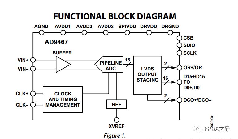
AD9467:
This is a 16-bit chip with a sampling rate of 250MSPS, as shown in the structural diagram below. VIN+/VIN- are the analog inputs, clk+/clk- are the clock signals for sampling the analog signal. D15+/D15- to D0+/D0- represent the converted data, and DCO+/DCO- is the clock signal output based on the data conversion.
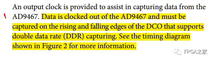
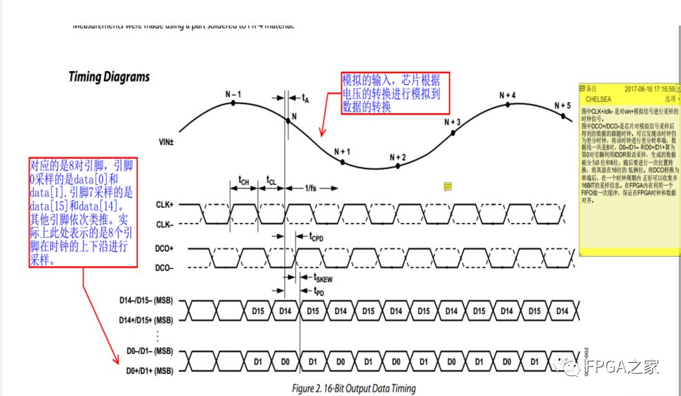
The chip performs the conversion from analog to digital based on the voltage. In the diagram below, one DCO clock cycle samples 16 bits of valid data. According to the chip manual, the data signal from the AD9467 must be captured at double the rate on both the rising and falling edges of the DCO. Refer to Figure 2.
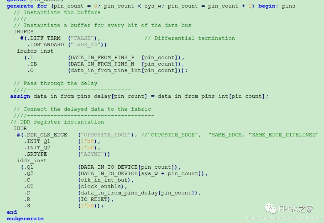
Based on the above diagram, in the FPGA program, we use the IBUFDS primitive to convert a set of data pins from differential to single-ended, and then use IDDR to double the data result and distribute it. For example, pin 0 is distributed to bits 0 and 8, while pin 1 goes to bits 1 and 9. However, pin 0 should actually be distributed to bits 0 and 1, so we swap the data positions in the outer module. The conversion for all 8 pairs of pins is done using the following code.
The DCO clock signal is processed with the following code. The incoming DCO differential signal is first converted to single-ended using IBUFGDS, then driven with the BUFIO primitive, and finally enters the BUFR primitive, which is mainly used to drive the sampling pins in the adjacent bank. The resulting clock signal is used as a follow-up clock for sampling the 16-bit data.
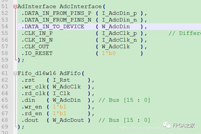
After converting both the data and clock, we store this data and clock in FIFO and read it using the same rate clock inside the FPGA to align the data with the internal clock of the FPGA.

The signal W_AdcDout obtained from the above code, which has 165 bits, is then reordered as shown in the following code.

The above code performs the reordering. In Figure 2, the order is D15, D14, where in the IDDR primitive, Q1 is D15 and Q2 is D14. The above code sorts the order, and we can see that a negation is performed at the highest bit position; the reason is shown in the following diagram.
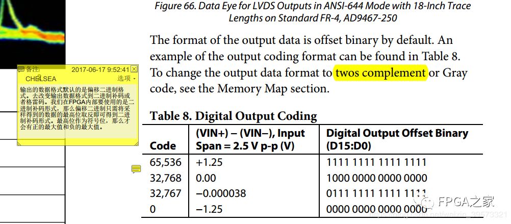
The output data format from the AD9467 is offset binary, and we need to convert it to two’s complement format for use inside the FPGA. The way to convert offset binary to two’s complement is to negate the highest bit. Thus, in the above code, negating the highest bit yields the corresponding two’s complement format for use in the FPGA. If a signal source is provided to the AD chip, a corresponding sine wave signal can be observed.
AD9640:
AD9640 is a 14-bit ADC and a dual-port AD chip.
Let’s look directly at the chip structure.

In the diagram, VIN+a/VIN-a and VIN+b/VIN-b are the two sampling ports A and B, using clk+/clk- for sampling.
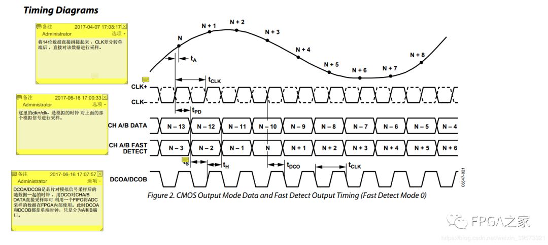
In the diagram, clk+/clk- is used for sampling the analog signal, CHA/B DATA represents the converted data for A and B, and DCOA and DCOB are the corresponding clock signals for the two data sets. In the next diagram, it can be seen that one clock cycle can directly sample the data. The default output format of the chip is offset binary, and negating the highest bit will yield the two’s complement format usable in the FPGA.
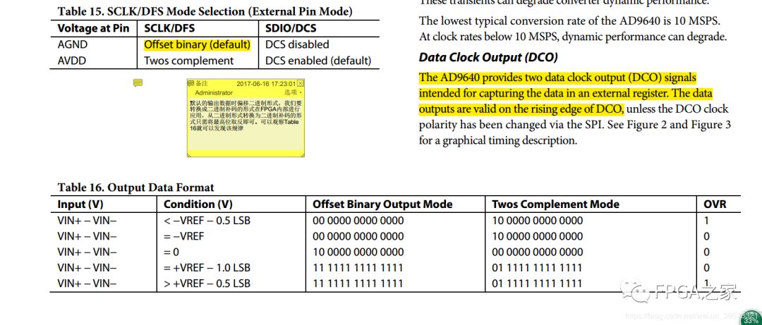
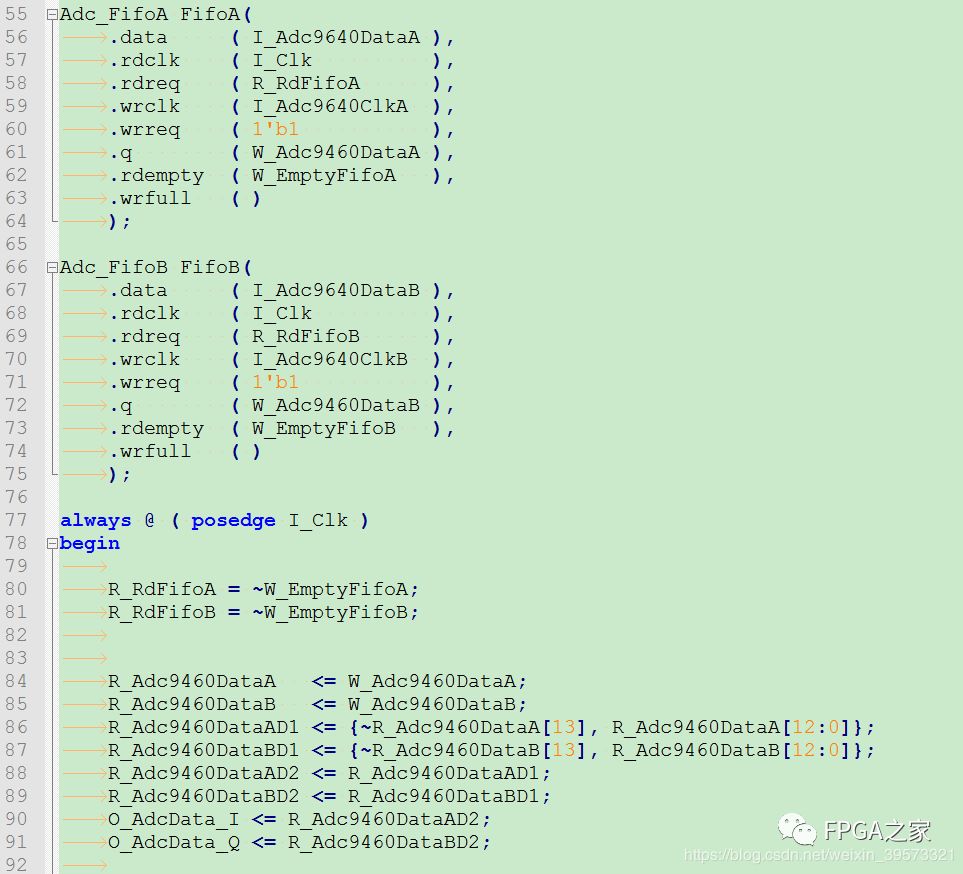
Using the above information, we can store the sampled data from AD9640 and the corresponding DCO clock in FIFO, read them with the same rate clock, and then negate the highest bit to obtain the two’s complement format.
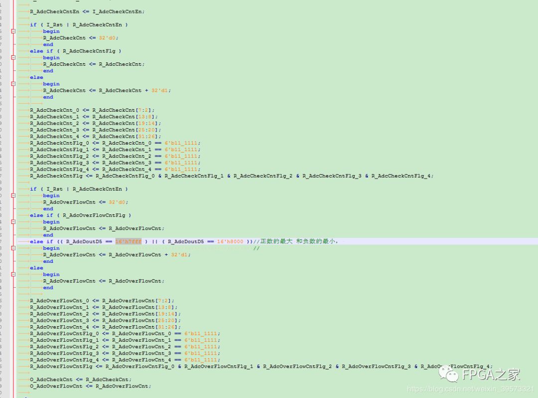
AD sampling may overflow. We use logic to detect the maximum positive value (16’h7fff) and the minimum negative value, counting their occurrences over a period. The detection counts and overflow counts are reported, serving as a basis for debugging the amplifier values. As shown in the diagram, counting starts after enabling, and both counters are reported.
Understanding DAC Chip Functions
AD9122:
AD9122 is a dual-channel, 16-bit, high dynamic range DAC that provides a sampling rate of 1200 MSPS and can generate multiple carriers up to the Nyquist frequency.
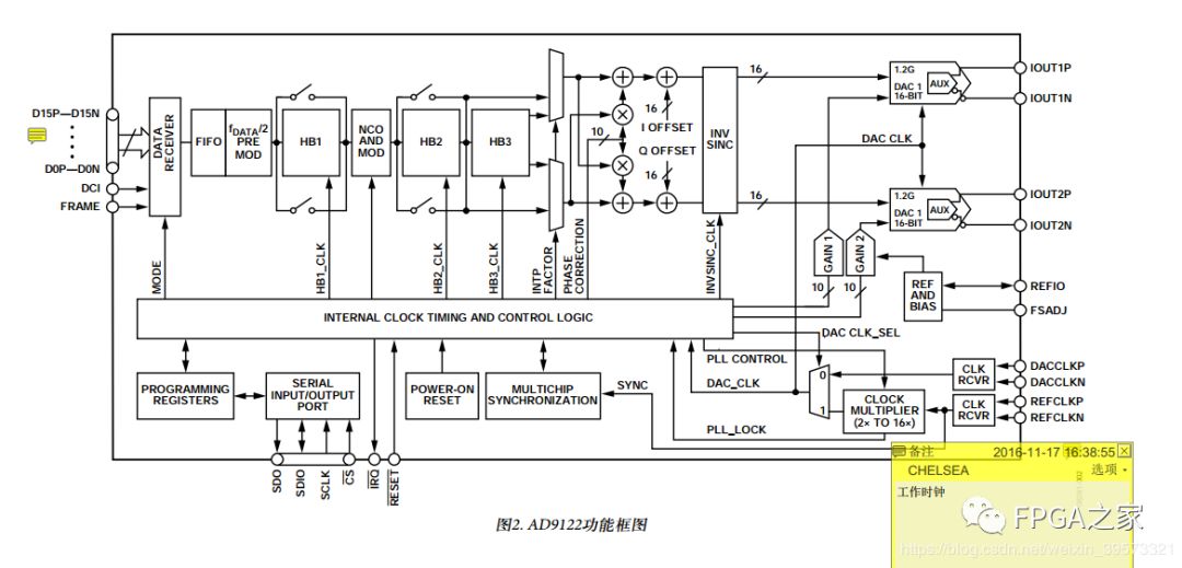
In the diagram, D15P~D0p and D15N~D0N are the data sent to the DA, and DCI is the clock signal accompanying the data. In byte and half-word modes, FRAME selects which channel to send the data to. IOUT1P and IOUT1N are the outputs for channel 1, while IOUT2P and IOUT2N are for channel 2. DACCLKP and DACACLKN are internal clock signals used by the chip, which can also use REFCLKP and RECLKN clock signals to supply the chip through internal frequency doubling. The frequency value of DACCLK is either the frequency of REFCLK after frequency doubling or directly provided by DACCLK.
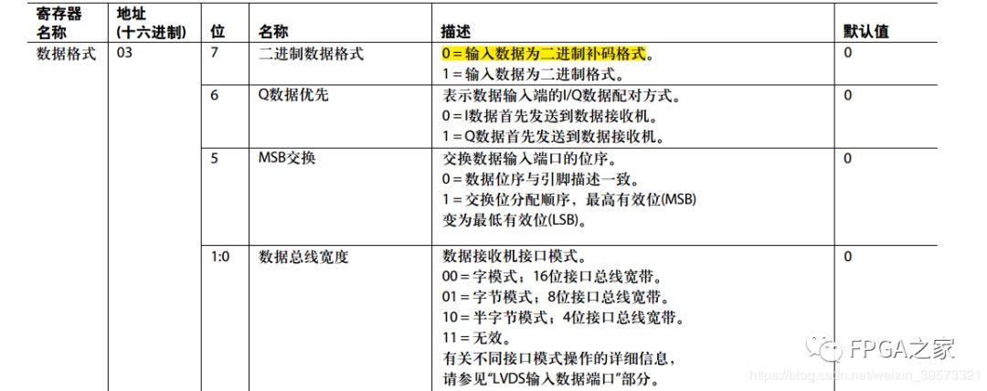
The data format can be configured through internal registers. Since the data generated by our FPGA internal DDS is in two’s complement format, we set this register to use the two’s complement format.
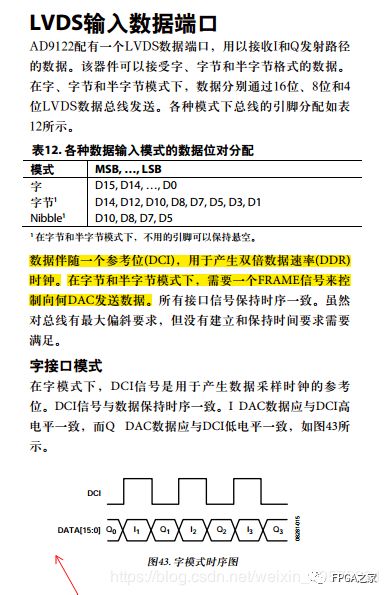
There are three styles for input data modes, and we selected the word interface mode. As seen in the diagram, the data is sent under a double-rate clock. Within one clock cycle, the IQ signals are sent in DDR format. The code is as follows.
In the above module, the clock clk_in_int_buf is 96M, sampling D1 and D2 at the rising and falling edges (also 96M), resulting in the data_out_to_pins_predelay rate of 192M. At this point, the format of the data sent to DA matches the diagram above. In the diagram, SAME_EDGE indicates that the data appears simultaneously on the data line, while OPPOSITE_EDGE indicates that data appears on the opposite edge, where D1 is sampled half a clock cycle earlier than D2. D1 is sampled at the rising edge, and D2 at the falling edge.
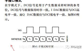
In the diagram, DCI is 96M, and DATA is 192M.
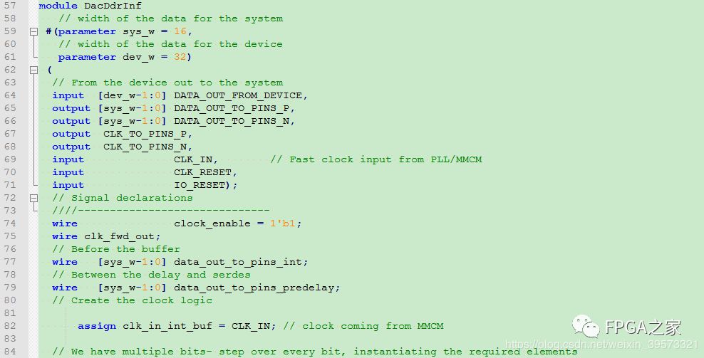
The top-level code is as follows. When inputting 32 bits, the real and imaginary parts are concatenated.
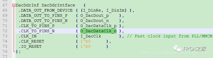
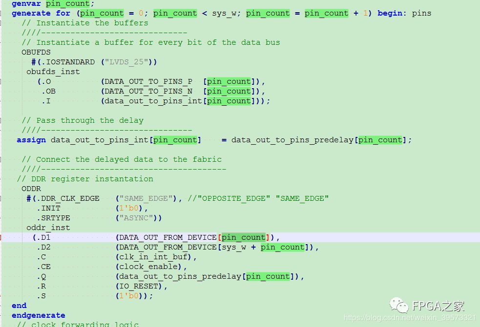
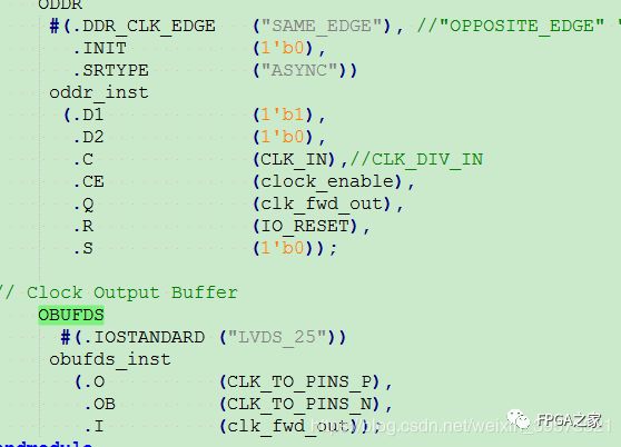
In the module, for example, the input of ODDR, DATA_OUT_FROM_DEVICE[pin_count] and DATA_OUT_FROM_DEVICE[sys_w + pin_count] extract the highest bit of the real and imaginary parts (assuming pin_count is 7) and form a DDR format data to send as a differential signal to the physical interface using OBUFDS. The same applies to clock operations, as shown in the diagram.
Here, CLK_IN is a 96M clock, sampling 0 and 1 at the rising and falling edges, resulting in clk_fwd_out being 96MHz.
DAC5672:
DAC5672 is a dual-port 14-bit DAC with a maximum sampling rate of 275MSPS.
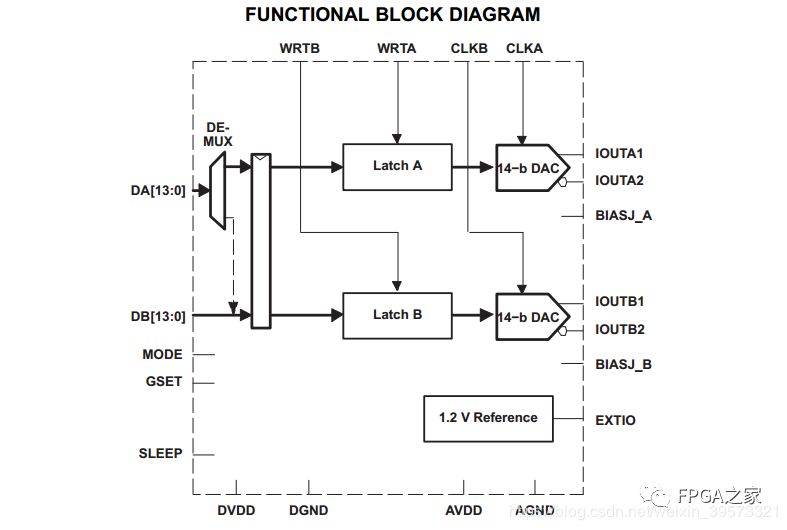
In the diagram, DA and DB are the data inputs for the two ports, and CLKA and CLKB are the clock signals corresponding to ports A and B.
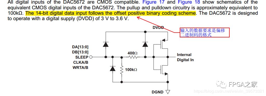
The chip requires the input data format to be in offset binary format.
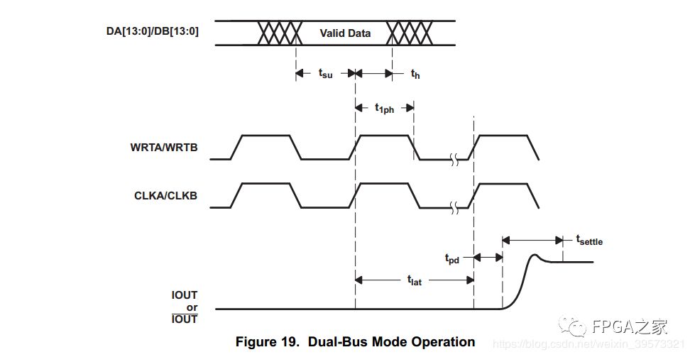
The two channels’ data are driven under the clock signals CLKA and CLKB.
The code part converts the highest bit of the input data from two’s complement format to the required offset binary format and connects the data to the corresponding physical pins.
2

Summary
The chip documentation mainly focuses on the input/output styles of the chip, followed by data formats, and finally data modes.
Disclaimer: