
01What is Kirchhoff’s Theorem?
Kirchhoff’s Current Law: The algebraic sum of currents entering and leaving any node in a circuit is zero.
Kirchhoff’s Voltage Law: The algebraic sum of voltages in any closed loop of a circuit is zero.
02Thevenin’s Theorem
A two-terminal circuit containing independent sources, linear resistors, and controlled sources can be equivalently represented as an ideal voltage source in series with an internal resistance model.
The value of the ideal voltage source is the open-circuit voltage between the two terminals of the active two-terminal circuit, and the series internal resistance is the equivalent resistance between the terminals when all independent sources are set to zero.
03Transistor Characteristic Curves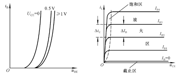 04Concept and Application of Feedback Circuits
Feedback refers to the process in an electronic system where a portion or all of the output (current or voltage) from an amplifier circuit is sampled through a feedback network and applied to the input loop in a certain way to influence the input quantity of the amplifier circuit.
Types of feedback include: voltage series negative feedback, current series negative feedback, voltage parallel negative feedback, and current parallel negative feedback.
Negative feedback has four effects on amplifier performance:
-
Improves the stability of the gain; as external conditions change (temperature, Vcc, device aging, etc.), the gain may vary, and the smaller the relative change, the higher the stability.
-
Reduces nonlinear distortion and noise.
-
Changes the input resistance (Ri) and output resistance (Ro) of the amplifier.
-
Effectively extends the bandwidth of the amplifier.
Characteristics of voltage negative feedback: The output voltage of the circuit tends to remain constant.
Characteristics of current negative feedback: The output current of the circuit tends to remain constant.
General principles for introducing negative feedback:
-
To stabilize the static operating point of the amplifier circuit, DC negative feedback should be introduced; to improve the dynamic performance of the amplifier circuit, AC negative feedback should be introduced (with polarity in the mid-frequency range).
-
If the internal resistance of the signal source is small or if a higher input resistance for the amplifier circuit is required, series negative feedback should be introduced; if the internal resistance of the signal source is large or if a lower input resistance is required, parallel feedback should be introduced.
-
Whether to introduce voltage or current negative feedback depends on the load’s requirements for the output quantity or output resistance of the amplifier circuit. If the load requires a stable signal voltage or a small output resistance, voltage negative feedback should be introduced; if the load requires a stable signal current or a large output resistance, current negative feedback should be introduced.
-
When signal conversion is needed, the appropriate configuration should be selected based on the functions of the four types of negative feedback amplifier circuits. For example, to achieve current-to-voltage signal conversion, voltage parallel negative feedback should be introduced in the amplifier circuit.
05Difference Between Active and Passive Filters
Passive Filters: These circuits are primarily composed of passive components R, L, and C.
Active Filters: Composed of integrated operational amplifiers and R, C, they have advantages such as no need for inductors, small size, and light weight.
The open-loop voltage gain and input impedance of integrated operational amplifiers are both very high, and the output resistance is low, providing certain voltage amplification and buffering effects when forming active filter circuits.
However, the bandwidth of integrated operational amplifiers is limited, making it difficult for current active filter circuits to operate at very high frequencies.
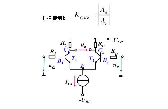
06Differential and Common Mode Signals
A pair of signals with equal magnitude and opposite polarity is called a differential mode signal; when a differential amplifier inputs a differential mode signal (uil = -ui2), it is referred to asdifferential input.
A pair of signals with equal magnitude and the same polarity is called a common mode signal; when a differential amplifier inputs a common mode signal (uil = ui2), it is referred to ascommon mode input.
In a differential amplifier, useful signals are input in differential mode, while interference signals are input in common mode, thus the interference signals will be suppressed significantly.
 07Comparison of FETs and Transistors
-
In environments with significant variations in conditions, field-effect transistors are more suitable.
-
Field-effect transistors are commonly used as preamplifiers to increase the input impedance of instruments and reduce noise.
-
Field-effect transistors have lower amplification capability than bipolar transistors.
-
They have a simple process, occupy less chip area, and are suitable for large-scale integrated circuits, finding broader applications in pulse digital circuits.
08Principles of Basic Amplifier Circuit Composition
-
The emitter junction should be forward-biased, and the collector junction should be reverse-biased.
-
The input circuit connection should ensure that the input signal is loaded onto the amplifier’s input terminal with minimal loss.
-
The output circuit connection should ensure that the output signal is transmitted to the load as much as possible.
09Conditions for Achieving Amplification
-
The transistor must be biased in the amplification region. The emitter junction should be forward-biased, and the collector junction should be reverse-biased.
-
The static operating point should be correctly set to keep the entire waveform in the amplification region.
-
The input circuit should convert the varying voltage into varying base current.
-
The output circuit should convert the varying collector current into varying collector voltage, filtering out only the AC signal through capacitors.
010Requirements for Power Amplifiers
-
The output power should be as large as possible.
-
High efficiency.
-
Low nonlinear distortion.
-
Transistor heat dissipation and protection.
011Frequency Compensation
Frequency compensation refers to the process of increasing or decreasing the strength of signals at a specific frequency to compensate for the weakening or enhancement of that frequency during signal processing. Common methods include negative feedback compensation, emitter capacitor compensation, and inductive compensation.
012Frequency Compensation in Amplifier Circuits
The purpose of frequency compensation in amplifier circuits is twofold: to improve the high-frequency characteristics of the amplifier circuit and to overcome the potential self-oscillation phenomenon that may occur due to the introduction of negative feedback, allowing the amplifier to operate stably.
In amplifier circuits, the presence of junction capacitance in transistors often leads to unsatisfactory high-frequency response. To address this issue, negative feedback is commonly introduced into the circuit.
However, the introduction of negative feedback can lead to new problems, such as self-oscillation, so frequency compensation must be performed to ensure the amplifier circuit operates normally and stably.
Methods of frequency compensation can be divided into lead compensation and lag compensation, primarily by incorporating some resistive and capacitive components to alter the open-loop gain’s phase-frequency characteristics at high frequencies. Currently, the most commonly used method is the phase-locked loop.
013Basic Amplifier Circuits
Function of Amplifier Circuits: Amplifier circuits are one of the most widely used circuits in electronic technology, serving to amplify weak input signals (voltage, current, power) to the required values for the load without distortion.
Types of Amplifier Circuits:
-
Voltage Amplifier: Designed to amplify small input signals to achieve a larger output voltage without distortion, also known as small-signal amplifiers;
-
Power Amplifier: Designed to amplify larger input signals to provide sufficient output power, also known as large-signal amplifiers.
A differential circuit is a circuit that has two input signals, and the difference between these two signals serves as the effective input signal for the circuit, with the output being the amplification of the difference between these two input signals.
Consider a scenario where interference signals affect both input signals equally; through their difference, the effective input of the interference signal becomes zero, achieving the goal of resisting common-mode interference.
014Class A, Class B, and Class AB Amplifiers 015Sketch the Block Diagram of a Phase-Locked Loop and Describe Its Principle
Phase Locking: Locking the phase and fixing the frequency at a specific value.
Phase-Locked Loop: A loop that locks the phase.
Components of a Phase-Locked Loop: Phase Detector (PD) + Frequency Divider + Loop Filter (LPF) + Voltage-Controlled Oscillator (VCO), etc.
Working Principle of a Phase-Locked Loop:
-
The output of the voltage-controlled oscillator is sampled and divided;
-
Simultaneously input to the phase detector with the reference signal;
-
The phase detector compares the frequency difference between the two signals and outputs a DC pulse voltage;
-
Controls the VCO to change its frequency;
-
Thus, after a short time, the output of the VCO stabilizes at a desired value.
Reference Signal:
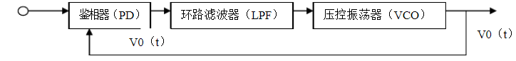
The phase detector is a phase comparison circuit that compares the reference signal input with the output signal from the VCO, outputting an error signal representing the phase difference. This error signal is filtered through the loop filter to remove harmonic and noise components, resulting in an error voltage that controls the VCO, causing the frequency of the voltage-controlled oscillator to change in the direction of reducing the frequency and phase difference between the two signals, ultimately making the output frequency of the VCO equal to that of the reference signal.
016Zero Drift
Zero drift refers to the phenomenon where, when the input of an amplifier circuit is shorted, there is still a slow variation in the output voltage, meaning the output voltage deviates from its original starting point and fluctuates up and down.
Methods to Suppress Zero Drift Generally Include:
-
Using constant temperature measures;
-
Compensation methods, using thermosensitive components to counteract changes in the amplifier or using matched amplifiers to form a differential amplifier circuit;
-
Using DC negative feedback to stabilize the static operating point;
-
Using resistive-capacitive coupling between stages or employing specially designed demodulating DC amplifiers, etc.
017Frequency Response
Frequency Response: Also known as frequency characteristics, frequency response is a technical indicator that measures the adaptability of an amplifier circuit to input signals of different frequencies.
In amplifier circuits, due to the presence of reactive components (such as capacitors, inductors, etc.) and junction capacitance in transistors, when the frequency of the input signal is too low or too high, the gain of the amplifier circuit will decrease, and phase lead or lag phenomena will occur.
In other words, the gain (or amplification factor) of the amplifier circuit is a function of the input signal frequency, which we refer to as the frequency response or frequency characteristics of the amplifier circuit.
Essentially, frequency response refers to the relationship between the amplifier’s gain and frequency, and a good amplifier should not only have sufficient gain but also good fidelity.
This means that the amplifier should have low nonlinear distortion and good frequency response, where “good” indicates that the amplifier should provide equal amplification for signals of different frequencies.
Causes of Frequency Response: One is that the actual amplified signal frequency is not singular; the other is that the amplifier has reactive components and factors.
Due to the presence of reactive components (such as inter-electrode capacitance, load capacitance, distributed capacitance, coupling capacitance, emitter bypass capacitance, etc.) in the amplifier circuit, the amplifier may have different amplification factors and phase shifts for different frequency signal components.
If the amplifier circuit amplifies signals of different frequencies with different amplitudes, it will cause amplitude distortion; if the amplifier circuit produces different phase shifts for signals of different frequencies, it will cause phase distortion.
Amplitude distortion and phase distortion are collectively referred to as frequency distortion. Since this distortion is caused by the linear reactive components (resistors, capacitors, inductors, etc.) of the circuit, it is not termed linear distortion. To achieve distortion-free signal amplification, it is necessary to study the frequency response of the amplifier.
The frequency response of an amplifier circuit can be described using amplitude-frequency characteristic curves and phase-frequency characteristic curves. If the amplitude-frequency characteristic curve of an amplifier circuit is a straight line parallel to the x-axis (or parallel to the x-axis within the frequency range of interest), and the phase-frequency characteristic curve is a straight line passing through the origin or a straight line passing through the origin within the frequency range of interest, then the frequency response is stable.
Methods to Change Frequency Response Mainly Include:
-
Changing the component parameters of the amplifier circuit;
-
Introducing new components to improve the existing amplifier circuit’s frequency response;
-
Adding new amplifier circuits in series to form multi-stage amplifier circuits.
018Transistor Operation in the Amplification Region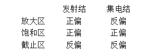 019Why Do Receivers Need AGC Circuits?
-
Received signals can vary greatly in strength; without AGC, the output will fluctuate significantly, affecting performance.
-
To receive weak signals, the gain of the receiver is usually set high, meaning high sensitivity. However, when receiving strong signals, if the gain of the channel is not adjusted, it can lead to adverse effects.
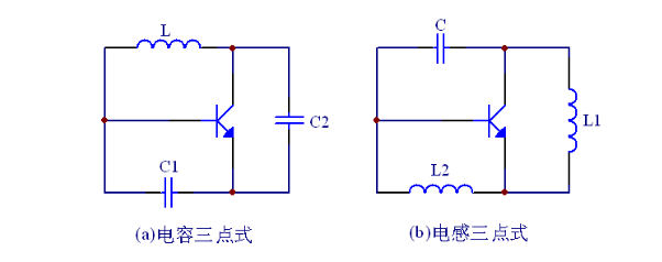
020LC Sine Wave Oscillator
Inductor-based and capacitor-based oscillators.
 021Phase Compensation in Differential Amplifiers
As the operating frequency increases, amplifiers may introduce additional phase shifts, potentially turning negative feedback into positive feedback and causing self-oscillation. Phase compensation can eliminate high-frequency self-oscillation.
The principle of phase compensation is to use a small capacitor C (tens to hundreds of microfarads) in the high-gain intermediate stage to form a voltage parallel negative feedback circuit, allowing for capacitive correction and RC correction to modify the phase-frequency and amplitude-frequency characteristics.
022Calculating Common Mode and Differential Mode Components in Differential Circuits
Let the common mode component be Yc and the differential mode component be Yd, then the outputs can be expressed as:
Y+=Yc+Yd
Y-=Yc-Yd
023Input and Output Resistance of Amplifiers
In amplifier circuits, it is generally desirable for the input resistance to be high, as this minimizes the impact on the signal source.
From the output side of the amplifier circuit, it can be equivalently represented as a signal source with a certain internal resistance, where the internal resistance is the output resistance. Typically, a lower output resistance is preferred to enhance the amplifier’s ability to drive loads.
024Principle of DC Voltage Regulators
Function:
To convert AC voltage into a stable and suitable DC voltage.
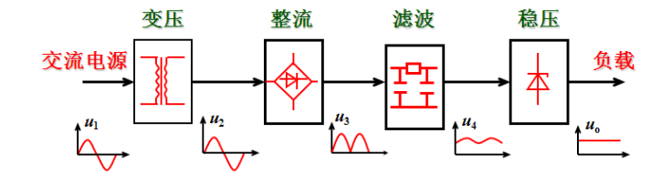
Power Transformer: Converts the AC grid voltage u1 into a suitable AC voltage u2.
Rectifier Circuit: Converts the AC voltage u2 into pulsating DC voltage u3.
Filter Circuit: Converts the pulsating DC voltage u3 into smooth DC voltage u4.
Voltage Regulator Circuit:
Eliminates the effects of grid fluctuations and load changes, maintaining the stability of the output voltage uo.
025Composition of Integrated Operational Amplifier Circuits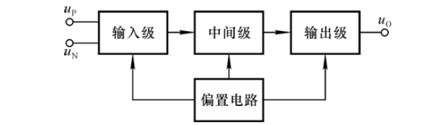
Bias Circuit:
Sets appropriate static operating points for each amplification stage, often using constant current source circuits.
Input Stage: Typically a differential amplifier circuit, requiring high Ri, large Ad, and small Ac, with high input voltage tolerance, having both in-phase and out-of-phase inputs.
Intermediate Stage: The main amplification stage is often a common-emitter amplifier circuit, typically using compound transistors, requiring sufficient amplification capability.
Output Stage: The power stage, often using complementary push-pull amplifier circuits or emitter followers, requiring low Ro, maximum undistorted output, and as large an output voltage as possible.
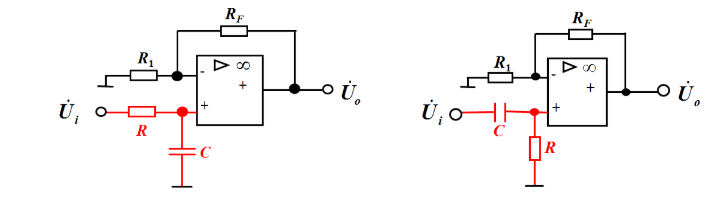
026Active Filters
First-order active low-pass and high-pass filters.
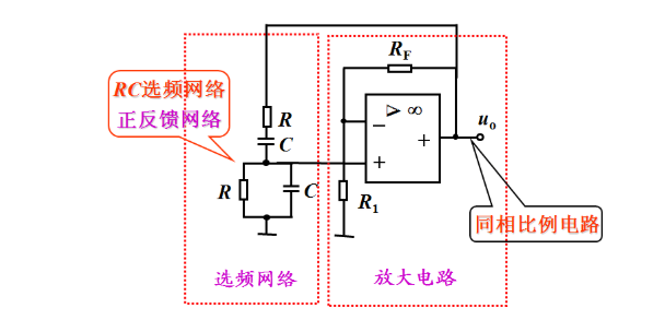
 027Composition and Working Principle of RC Oscillators
Components of Sine Wave Oscillator Circuits:
-
Amplifier Circuit: Amplifies the signal.
-
Feedback Network: Must be positive feedback, where the feedback signal is the input signal to the amplifier circuit.
-
Frequency Selection Network: Ensures the output is a single frequency sine wave, even if the circuit only meets its oscillation conditions at a specific frequency.
-
Amplitude Stabilization Component: Allows the circuit to transition from ½AuF½ >1 to ½AuF½ =1, achieving stable amplitude oscillation.


Some Screenshots of Electronic Books

Some Screenshots of Course PPTs

【Complete Set of Hardware Learning Materials】