What is a Reticle (Photomask/Mask)?
Reticles and photomasks are collectively referred to as PhotoMasks (including Reticle, Mask).
•[Mask,Pellicle (protective film),DUV,ArF,I-line,EUV,reflective masks]
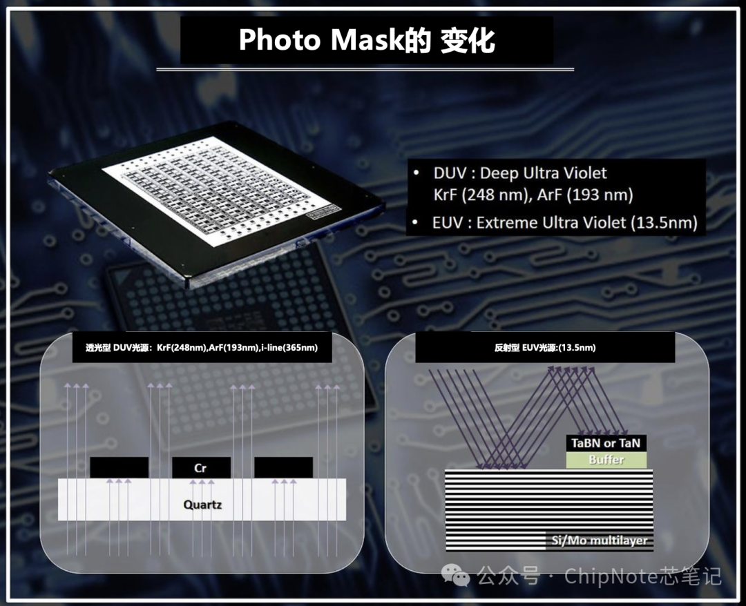
Reticle is a photomask that contains the designed pattern in the lithography process. The detailed structure of the mask includes a Pellicle (thin polymer functional film) and a quartz glass plate, and it blocks incident light through a chromium (Cr) coating over the entire pattern area, allowing only the desired graphic parts to be transparent.
In the DUV region, which includes I-line (365nm),KrF (248nm),ArF (193nm), a transmissive mask is used; while for EUV (13.4nm), due to the shorter wavelength, most of the energy is absorbed by the mask, thus a reflective mask is used.
Reflective masks in EUV.
EUV uses a quasi-monochromatic light source with a wavelength of 13.4 nm. Due to the high energy of the light source, if a transmissive mask is used, energy absorption occurs, making it difficult to achieve the desired pattern. To reduce absorption, a very thin mask layer is required, but this makes it challenging to form ideal graphics, thus presenting challenges.
Therefore, a Si/Mo multilayer structure is used to form the reflective layer, achieving a reflective mask that reflects the desired image pattern like a mirror.
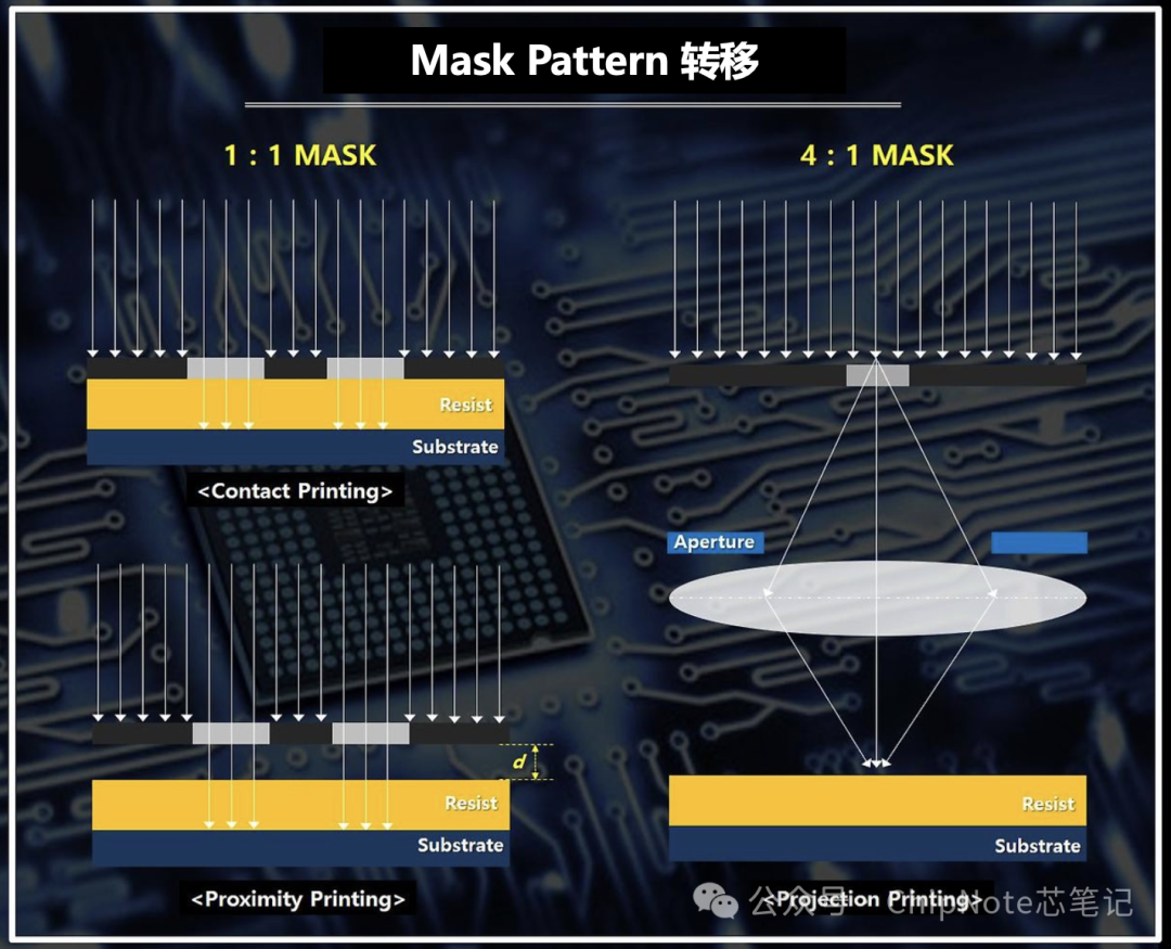
Methods for transferring the mask pattern.
[Proximity, Projection, Electron Beam Exposure (e-beam lithography)] methods transfer the image pattern from the mask to the wafer. The transfer methods can be classified as 1:1, 4:1, 5:1, etc. In semiconductor lithography, although the goal is to transfer the mask pattern to the wafer in proportion, a more important goal is to transfer the image pattern after reduction (reduction projection). Proximity printing (1:1) was used in earlier stages but is no longer used for mass production; instead, 4:1 or 5:1 reduction projection methods are adopted. Masks are typically made using electron beam exposure (e-beam lithography), which does not require traditional masks and can generate basic patterns based on 3D CAD designs, and then the enlarged pattern is reduced by 1/4 or 1/5 through a Projection lens and projected onto the wafer for printing. “Contact” and “Proximity” printing methods refer to the methods where the mask pattern and the transferred pattern on the wafer are in a 1:1 ratio. Although not used in mass production, they can be seen in research units using Mask Aligner equipment. Contact printing has issues with mask contamination, while Proximity types have scattering issues due to light not penetrating the mask.
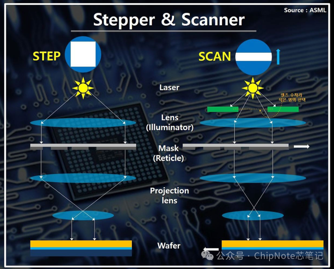
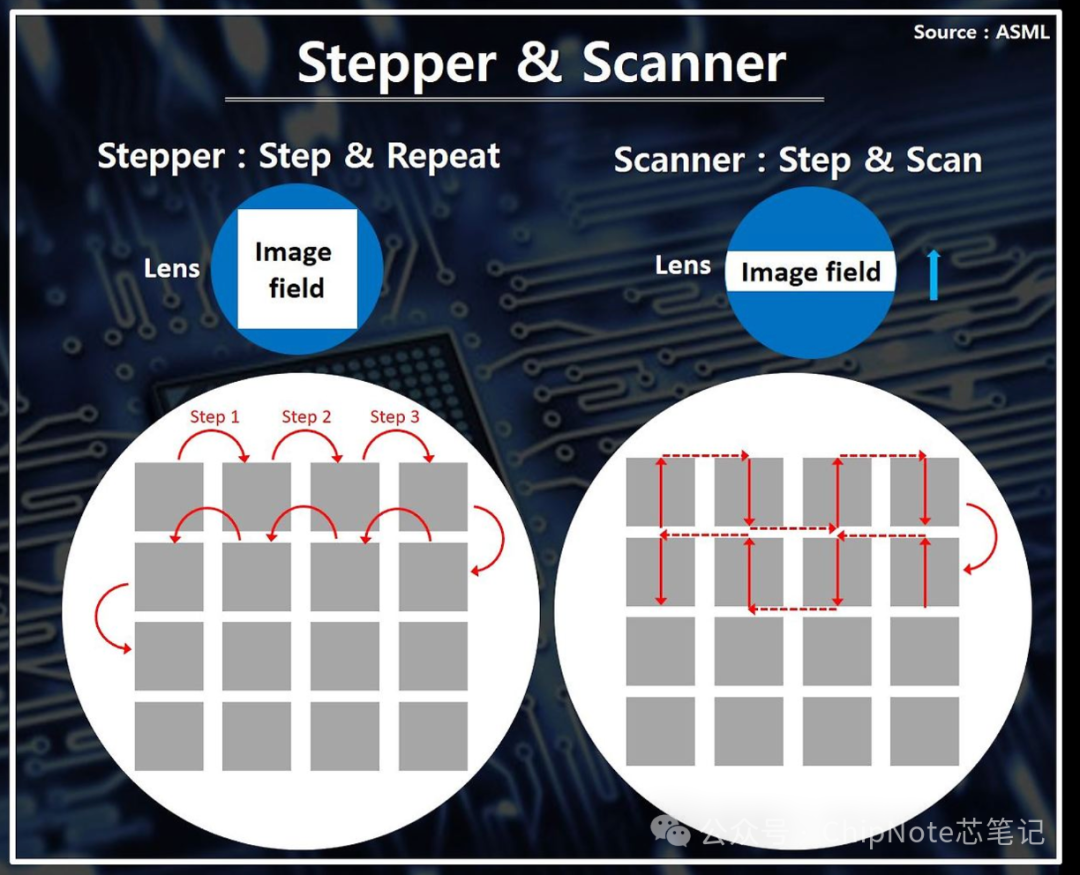
Differences between Scanner and Stepper.
Scanner (Step & Scan) and Stepper (Step & Repeat), numerical aperture, projection lens are the core equipment in the lithography process, with Scanner being the primary device. However, Stepper types also exist. When light is scanned while moving, it is referred to as a “Step & Scan” type Scanner; while exposing an image all at once on the wafer is a “Step & Repeat” type Stepper. However, Stepper cannot image the entire mask image at once, especially at the edges of the lens where aberrations or distortion may occur, making it difficult to transfer the image accurately. To overcome this limitation, the current method is to project and scan image quality from the best, most stable light regions of the lens.
The structure of the Scanner. The Scanner structure consists of an external sealed chamber. Inside, it includes a mask (Mask) and Excimer laser light sources such as KrF, ArF, etc., with the laser entering the system through the optical path. Through the projection lens, the light is correctly focused and transmitted onto the silicon wafer. The light entering the Reticle contains pattern information, which is reduced by 1/4 through the projection lens before reaching the wafer, which is the basic imaging principle. To ensure that light can accurately reach the wafer, more than 30 sets of projection lenses are typically used. The projection lens consists of a condenser lens used to collect divergent light and an objective lens that focuses the pattern light onto the wafer.
“Aberration” refers to the phenomenon where light that should converge on the same plane cannot accurately converge at a point, resulting in blurriness and diffusion. Due to the geometric shape of the lens or mirror causing differences in the light path, image distortion or blurriness occurs, which is called “optical aberration.” One important reason for replacing Stepper with Scanner is to overcome this aberration issue.
Definition of Photo Mask:
A high-precision disk with a precise circuit pattern.
It is the basic raw material in the semiconductor lithography process, deposited with a light-blocking film on a quartz (Qz) substrate to form circuit patterns.
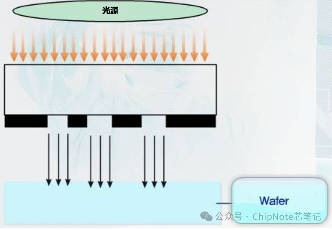
Uses of Photo Mask – Used as raw material required for lithography in wafer processing.
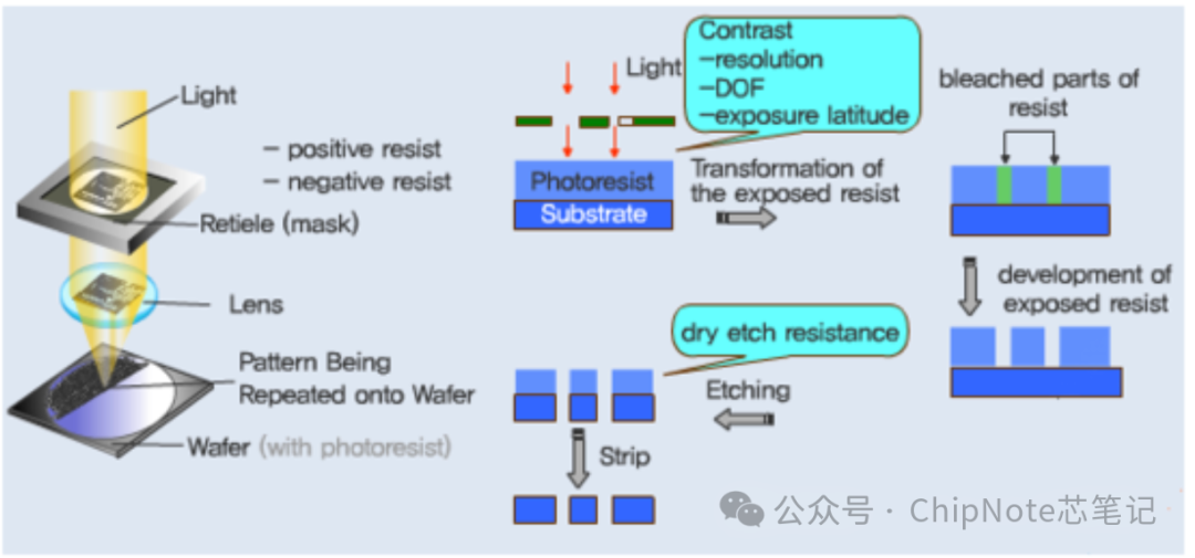
The principle is similar to that of camera developing film – by making a master (photomask), the same pattern shape can be reproduced consistently.
The basic structure of Photo Mask – a light-blocking film is deposited on a quartz substrate, and a pattern shape is formed on it.
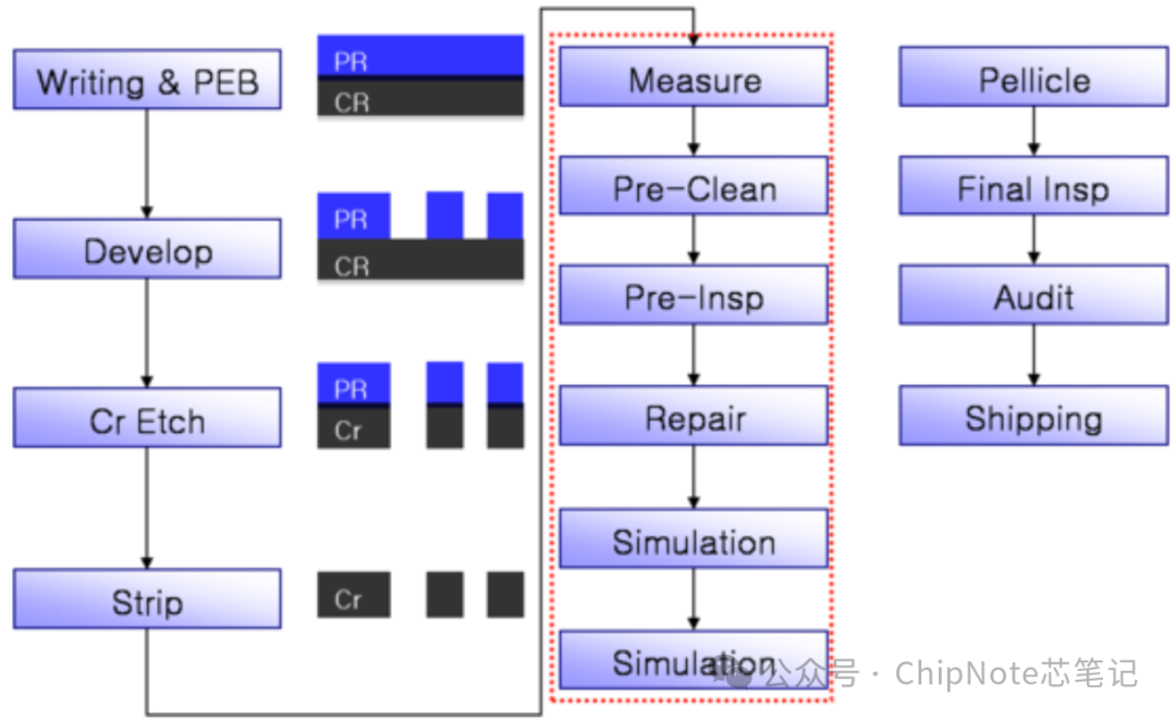
Substrate: using quartz / Light-blocking film: using chromium (Chrome)
Light-blocking film: a thin layer used to block light from passing through (usually using chromium).
Types of Photo Mask – can be classified based on usage purpose, photoresist type, exposure equipment, structure, thickness, and size.
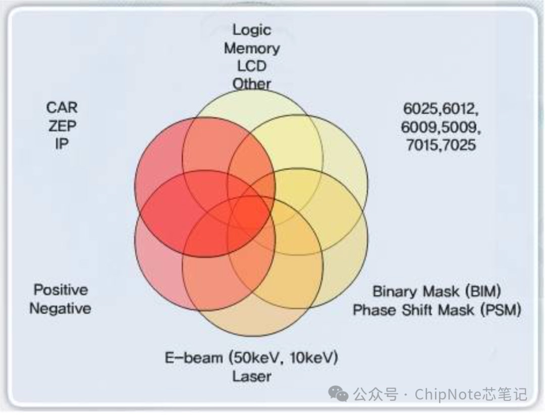
* Resolution
To improve the integration of semiconductor devices in recent years, it is necessary to reduce the minimum line width achievable → thus, improving resolution is very important.
Resolution = K1 × λ / NA
•λ = wavelength of the exposure light source
•K1 = process constant
•NA = numerical aperture
* Factors related to resolution include:
•In wafer processing, the wavelength used in lithography related to the performance of the Stepper and numerical aperture (NA), and the role of photoresist and further improvements to the Photo Mask are also very important.
* RET (Resolution Enhancement Technology): technology to enhance resolution.
•Short wavelength light sources (development of light sources and optical systems)
•Reducing K1 value (development of processes and photoresists, improvement of masks)
•Increasing NA (improving lens design)
•PSM (Phase Shift Mask), Phase Shift Mask
* OPC (Optical Proximity Correction)
→ Optical proximity effect correction technology (for improving pattern transfer accuracy).
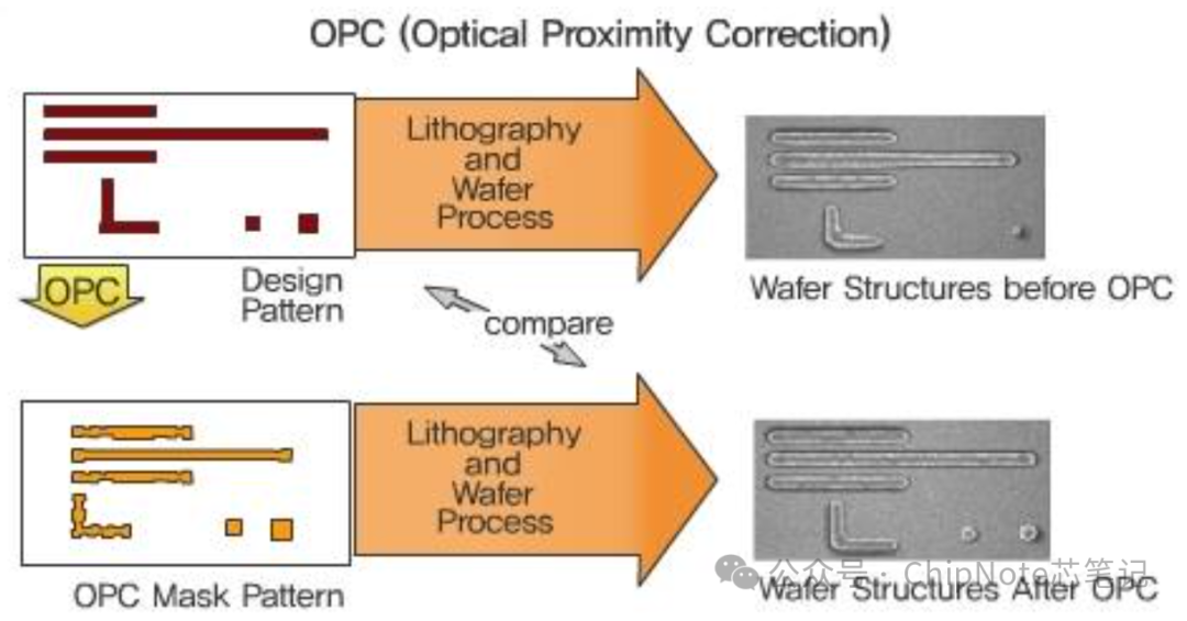
Types of OPC patterns.
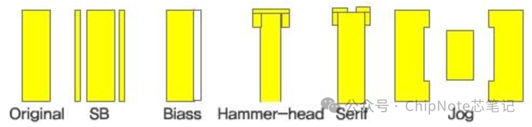
In the technology of improving resolution, it is widely used together with Phase Shift Masks.
Proximity Effect: refers to the phenomenon where the designed circuit pattern cannot be perfectly reproduced during the actual lithography process.
→ The main reason is the interference and diffraction effects of light, leading to reduced graphic sizes or rounded pattern edges.
Proximity Effect Correction (OPC):
Compensating for the above proximity effects by modifying the graphics in advance (such as using specific OPC pattern types).
PSM (Phase Shift Mask)
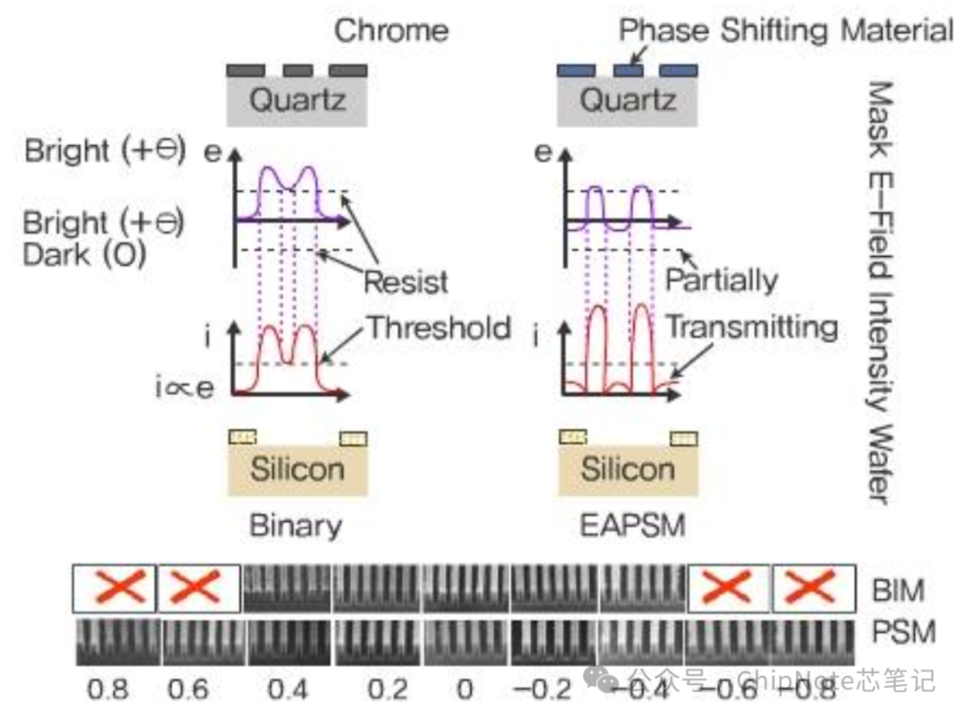
•Among various RET technologies, the most well-known in the field of masks (Photo Mask) is a RET technology that uses the interference phenomenon of light to enhance resolution, which is the Phase Shift Mask.
•Unlike general masks, to achieve phase reversal, a special phase-shifting layer is used.
•When the light passing through this phase-shifting layer has a 180-degree phase difference with the light passing through the ordinary quartz substrate,
•the intensity gradient area at the pattern edge will be reduced due to coherent interference, enhancing the contrast of the light intensity at the pattern edge and improving resolution.
•This technology is now widely used in the field of resolution enhancement in semiconductor device manufacturing.
Construction and requirements of Blank Mask.
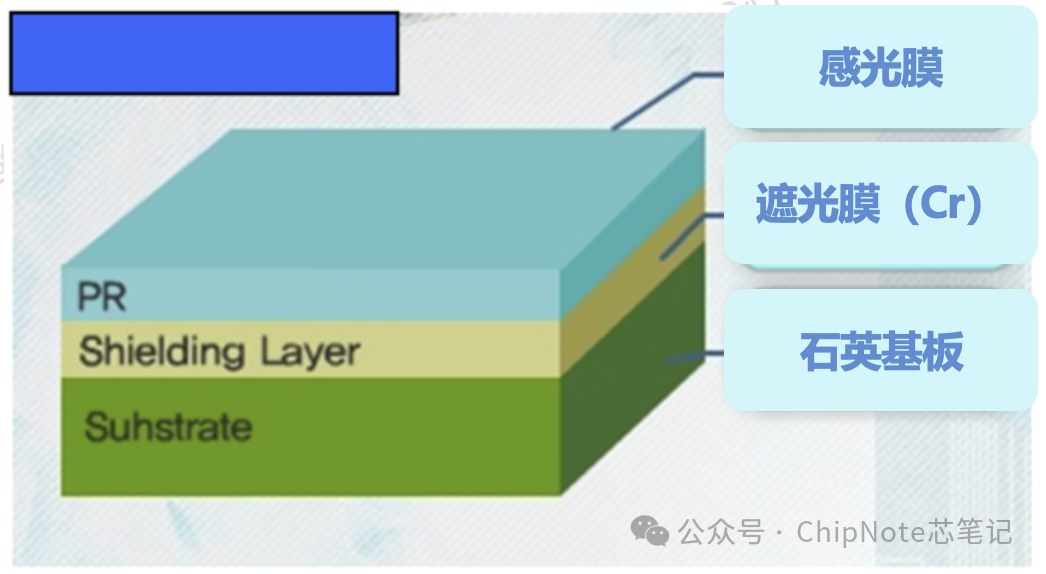
Low Thermal Expansion coefficient
Ensures that even when heated during exposure, the pattern size remains stable.
High Transparency (Quartz area)
In the quartz substrate area, it must have high transmittance to the exposure light source (such as i-line, KrF, ArF, etc.) to ensure clear pattern transfer.
Mechanical and Chemical Durability (Durability)
Can withstand physical and chemical stresses during processes such as cleaning, etching, and inspection, and is not easily scratched or deformed.
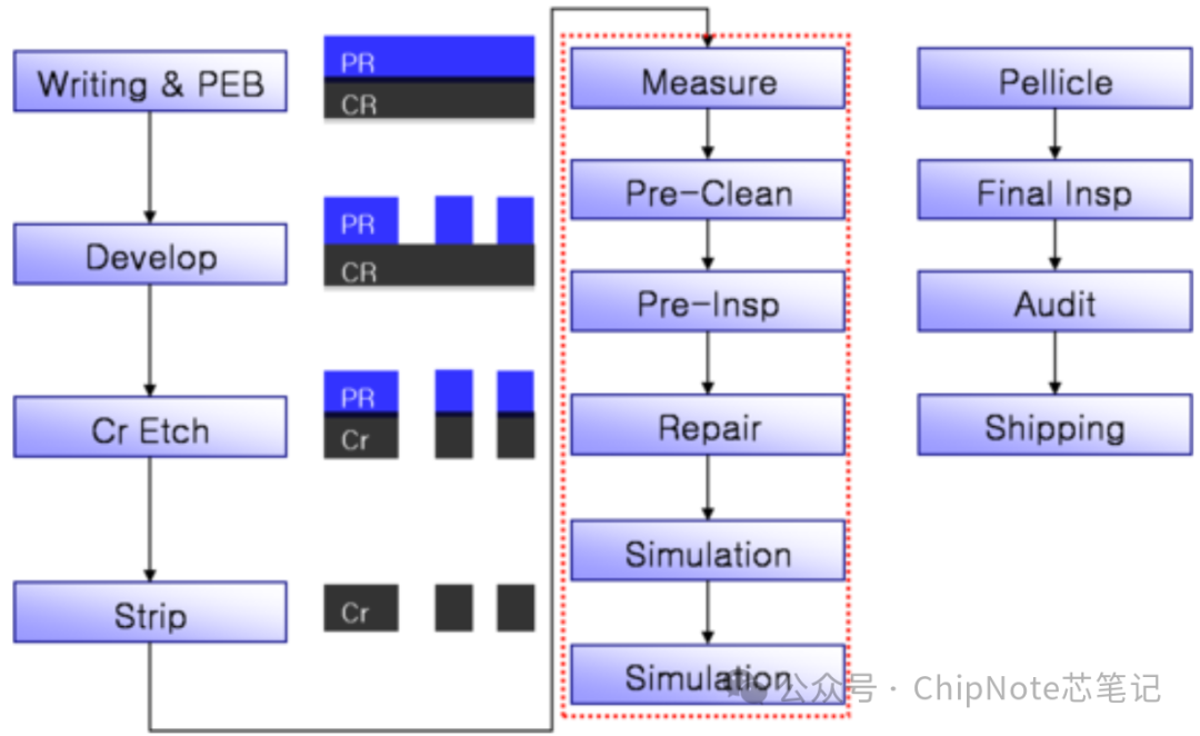
Basic Photo Mask Manufacturing Process:
-
Blank Preparation (including quartz substrate + Cr light-blocking film)
-
Coating
-
Pattern Writing – commonly using electron beam (E-Beam) or laser
-
Prebake (PEB)
-
Developing
-
Chromium Layer Etching
-
Stripping
-
Cleaning and Pellicle Packaging
-
Inspection & Repair
-
Final Quality Inspection and Shipment
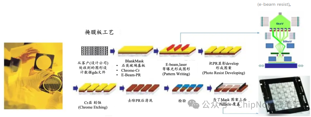
Photomask is a mask drawn on a quartz glass plate (Quartz) that allows ultraviolet light to pass through smoothly, using a light-blocking film (usually a chromium thin film, Cr) to draw the required pattern.
There is no “upper-level mask” in the process of making photomasks, so it is processed using the already completed chromium (Cr) coating and photoresist (PR) coated Blank Mask as the starting material.
The generation of patterns does not rely on the original photomask but is directly exposed on the photoresist through CAD, GPS data controlling electron beam direct writing (E-beam Direct Writing). After developing, the photoresist in the pattern area is removed, revealing the desired pattern. Then, the Cr layer is etched, and the remaining PR is removed (stripping) to complete the mask production.
* Additionally, in the final stage of photomask production, a protective cover called Pellicle is applied to its edges to protect the surface pattern of the mask from direct contamination by dust and other pollutants. Pellicle is a thin film with extremely high light transmittance,
which can isolate particles that fall on its surface from the focal plane during the lithography process, ensuring clarity of pattern projection and process stability.
– The manufacturing process of photomasks is similar to the lithography process of wafers.
•Writing & PEB: Since it is a point-by-point drawing process, it is called a Writer (writing machine).
•Develop: Selectively develop the exposed areas of the photoresist.
•Cr Tech: Using photoresist as a mask, selectively etch the light-blocking layer of the chromium layer.
•Strip: Remove unnecessary photoresist.
•→ Thus, the basic mask is completed, followed by measurement and inspection processes for quality confirmation.
* Unit process (lithography) – Writing (exposure drawing)
• This is the process of writing the designed circuit diagram onto the mask.
•→ Unlike the “expose” in wafer processing, this is specifically referred to as the writer
• Change the molecular structure or composition of the photoresist through lithography.
• The energy source required for photoresist exposure (light source): laser / electron beam.
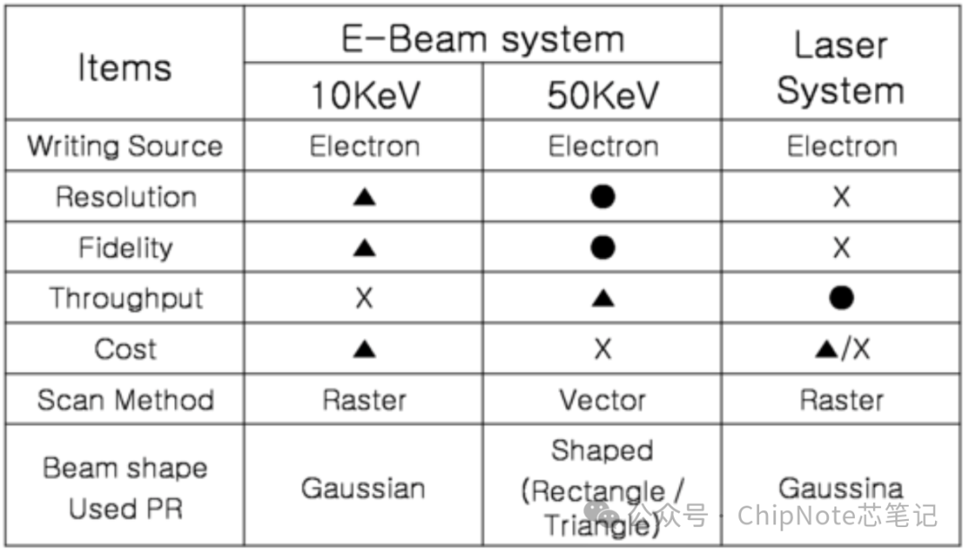
•E-Beam (electron beam) exposure is divided based on energy levels: 10KeV and 50KeV.
•→ Because electron beam lithography equipment has advantages in resolution and precision,
• it is the mainstream choice for products with high integration requirements.
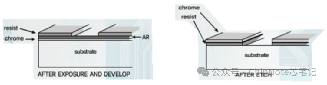
Unit Process (Develop) – Develop
The process of using a developer to remove the exposed areas of the photoresist.
Unit Process (Etch) – Etch
The process of using photoresist as a mask to remove the light-blocking layer (Cr layer) beneath the developed area.
Etching methods include:
Dry Etching
Wet Etching
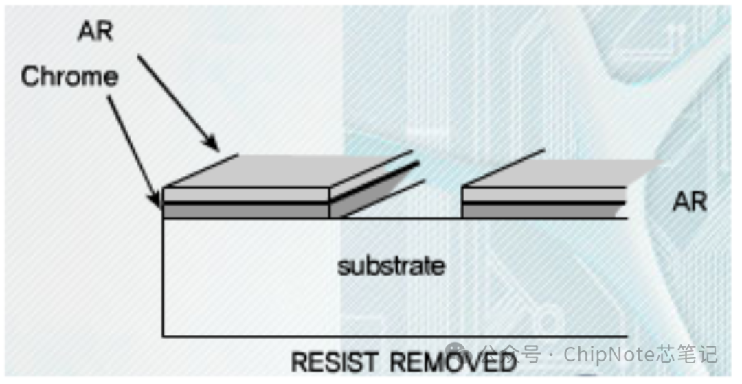
Unit Process (Strip) – Strip
After etching is completed, the process of removing the remaining unnecessary photoresist on the mask..
Usually treated with sulfuric acid (H₂SO₄);
In recent years, plasma-based stripping processes (Ashing) have also been commonly used for removal.
Unit Process (Cleaning) – Cleaning – Cleaning
• Use chemicals and water to remove impurities on the mask surface.
• Cleaning methods: 1.SPM (sulfuric acid (H₂SO₄) + hydrogen peroxide (H₂O₂) mixture) = Piranha: used to remove heavy organic matter.
2.Rinse (QDR (Quick Dump Rinse) + QFR (Flood Rinse)): neutralize larger particle acid residues.
3.SC1 (Standard Clean-1) = APM (ammonium hydroxide (NH₄OH) + hydrogen peroxide (H₂O₂) + water (H₂O)): removes surface acidic contamination caused by H₂O₂.
4.Megasonic: removes particles through vibration and cavitation energy.
5.IPA dry: removes deionized water (DI water) used in the cleaning process using hot vapor IPA (isopropanol).
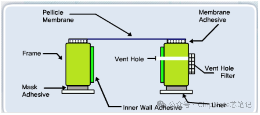
* Unit Process (Mask Film Protection Layer) – Pellicle – Pellicle
• After the final cleaning process, to prevent contamination of the mask surface, a thin film is applied to the mask surface.
•Pellicle structure: Frame / Membrane / Adhesive / Vent-hole.
•→ The role of Pellicle is:
• In the space between the mask and the lithography area, through heat and pressure differences, the membrane expands and contracts to prevent external air from entering, maintaining cleanliness during the lithography process.
• In some cases, by sealing pores with the membrane layer, it prevents air and particles from entering.
Quality Control of Photo Mask
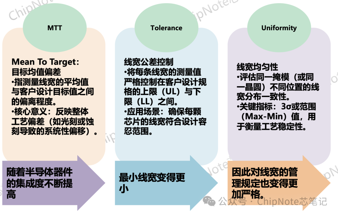
Line Width (Critical Dimension: CD)
Refers to whether the actual size of the pattern observed on the mask is consistent with the design size,
an important indicator for measuring pattern fabrication accuracy.
Defects – If there are defects in the photomask,
these defects will be transferred onto the wafer, potentially causing functional defects in the actual devices.
Chromium defects:
Refers to the residual chromium layer in areas that should be transparent, causing light to be unable to pass through normally.
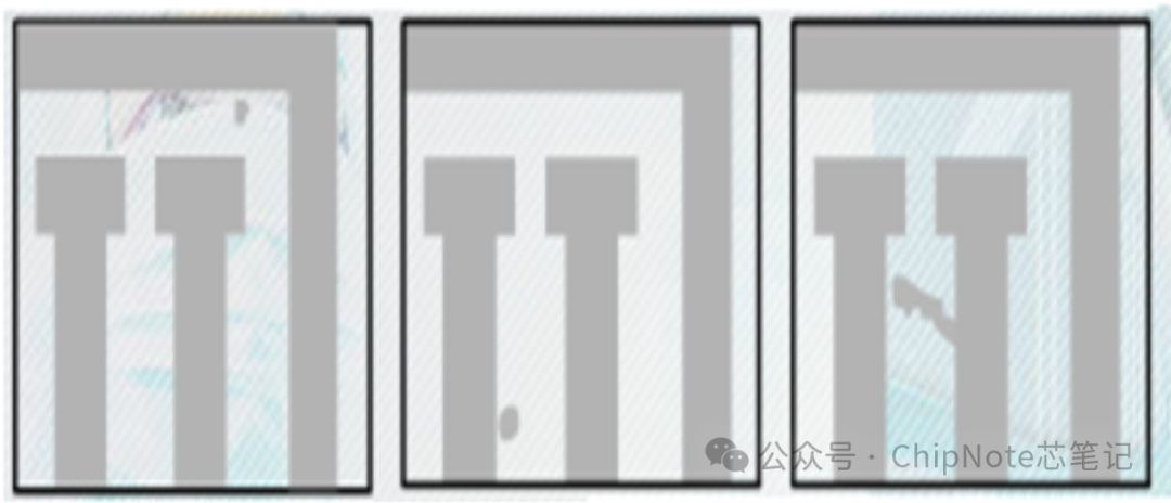
Clear defects:
Refers to the absence of a chromium layer in areas that should block light, causing light to pass through unexpectedly.
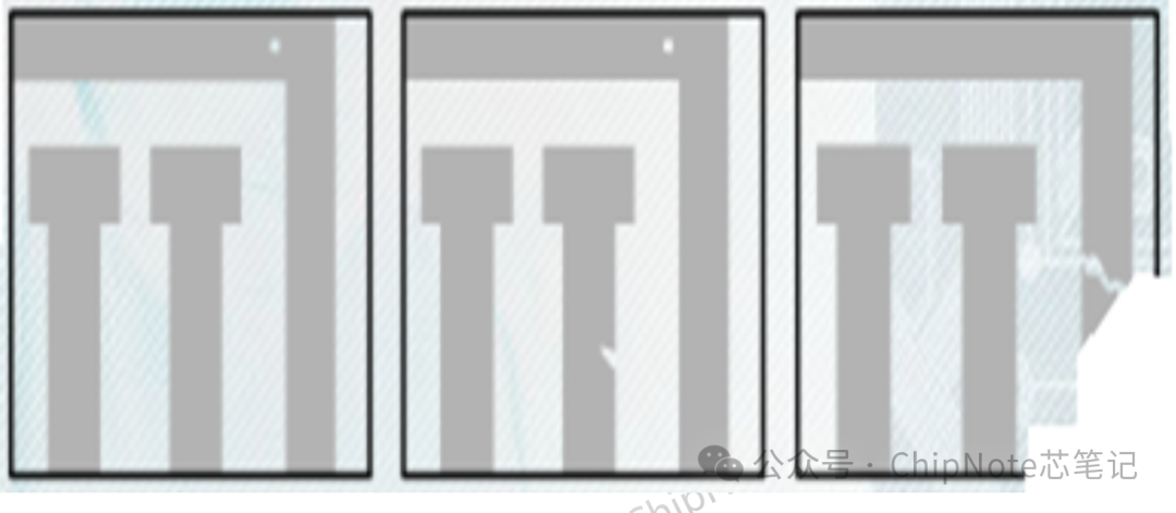
The inspection process that must be performed in the photomask (Photomask) process to determine if there are defects:
1.Pattern Inspection:
2. Check for subtle defects in the pattern.
3.Die to die inspection.
4.Die to DB (Database) inspection.
5. Inspect for particles on the mask surface or Pellicle membrane surface.
6. Mainly using dedicated inspection equipment to detect particles.
7. If particles are present, it will cause scattering issues.
8. Visual inspection, microscope inspection.
9. Mainly used to detect larger defects.
* For defects found during inspection, the following repair processes are performed:
• Chromium layer defects: repaired using laser or gas cutting.
• Clear area defects: repaired by depositing material.
• Particles on the surface or Pellicle membrane: re-cleaning or using nitrogen to blow away particles.
* Alignment Detection (Registration)
• Measure the degree of deviation between the actual photomask pattern and the position it should be in according to the customer design.
• Why alignment is important:
• Because in wafer manufacturing, processes are performed according to multi-layer structures,
• each layer uses different masks, and alignment accuracy directly affects stacking accuracy.
Methods of expressing alignment accuracy:
Die-fit: Accuracy of the position of each chip unit (Die).
Run In/Out: Accuracy of the spacing (Pitch) between chip units.
Scale: Accuracy of long-distance spacing (Long Pitch).
Orthogonality: The vertical deviation between the X-axis and Y-axis of the pattern.
Overlay: The relative position accuracy between the current layer pattern and the previous layer pattern.
* Content of knowledge points edited by the team. If you are satisfied, please follow me.
Your attention is my motivation. Thank you*
[Introduction to Semiconductors] Semiconductor Product Development Process from Design to Production (Chip Design Sequence)
[Power Semiconductors] Trends in Vertical Structure GaN Power Semiconductor Technology for Electric Vehicle Applications
[Power Semiconductors] Power Semiconductor Discrete Devices and Integrated Circuits
[Mobile Communication Chips] (Surface Acoustic Wave Filters for Mobile Communication)
[First Communication Chip] 5G Era Innovation: The Rise of Next-Generation RF Chips POI-SAW and TF-SAW, Challenging the Dominance of Traditional SAW/BAW Filters!
[Second Communication Chip] 5G Era Innovation: The Rise of Next-Generation RF Chips POI-SAW and TF-SAW, Challenging the Dominance of Traditional SAW/BAW Filters!
[Display Production] Teaching You How to Use TFT-LCD Production Methods
Chip Processing (FAB): Special Gases (Gas) in Semiconductors