PCBs (Printed Circuit Boards) are the “nervous system” of electronic devices, mechanically securing and electrically connecting electronic components (such as chips, resistors, capacitors, etc.) through preset copper foil circuits and pads, replacing traditional manual soldering of wires. They are an indispensable core carrier of modern electronic devices.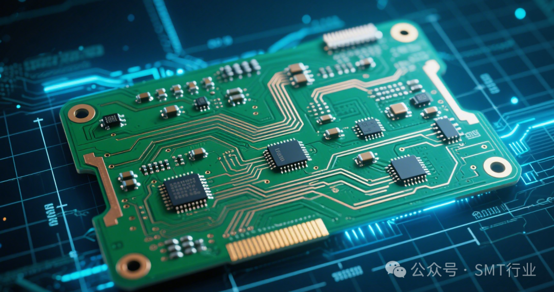 1. Core Characteristics of PCBs: Why They Are the “Standard Configuration” for Electronic Devices
Compared to the early “wire connection” method, the advantages of PCBs lie in their integration, standardization, and miniaturization, specifically reflected in three aspects:
1.Strong electrical stability:
The copper foil circuits are precisely etched by machines, with uniform line width and spacing, avoiding poor contact and short circuit risks associated with manual wiring, resulting in more stable signal transmission (especially for high-frequency signals);
2. High space utilization:Can be designed as single-layer, double-layer, or multi-layer (such as 4-layer, 6-layer, 12-layer), with components mounted on both sides of the board (SMT technology), significantly reducing device size (such as mobile phone motherboards, laptop motherboards);3. Low mass production costs:Standardized production processes (design → board manufacturing → soldering) can be replicated in bulk, suitable for large-scale electronic device production, and during maintenance, components can be quickly located through “silkscreen markings” (such as R1, C2, U1).
2. Main Classifications of PCBs: Based on Structure and Process
Different electronic devices in various scenarios have different requirements for the number of layers, materials, and processes of PCBs. Common classifications are as follows:
| Classification Dimension | Specific Type | Core Characteristics | Applicable Scenarios |
|---|---|---|---|
| By Number of Layers | Single-Layer PCB | Only one side has copper foil circuits, simple structure | Low-cost simple devices (such as toys, remote controls, power adapters) |
| Double-Layer PCB | Both sides have copper foil, connected through “vias” | Medium complexity devices (such as routers, small sensors, home appliance control boards) | |
| Multi-Layer PCB | 3 layers or more, including “inner layers” (power layer, ground layer), high wiring density | High complexity, miniaturized devices (such as mobile phones, computer CPU motherboards, automotive electronics, industrial controllers) | |
| By Process | Rigid PCB | Substrate made of rigid materials (such as FR-4 epoxy resin glass cloth), fixed shape | Most electronic devices (mobile phones, computers, televisions, SMT equipment motherboards) |
| Flexible PCB (FPC) | Substrate made of flexible materials (such as polyimide), can be bent and folded | Scenarios requiring adaptation to spatial deformation (such as mobile phone screen flex cables, smart watch motherboards, automotive wiring harness replacements) | |
| Rigid-Flex PCB (RFPCB) | Rigid parts for fixed components, flexible parts for bending connections | High integration, complex spatial devices (such as drones, medical devices, high-end automotive electronics) |
3. Core Uses of PCBs: The “Electronic Cornerstone” Across All Industries
The applications of PCBs span almost all electronic fields, from consumer electronics to industrial, medical, and automotive sectors. As long as there is a need for “electronic component connections,” PCBs are required as carriers. Specific scenarios can be divided into six major categories:
1. Consumer Electronics: The Most Common Application Scenario
- Core RequirementsMiniaturization, high integration, low cost;
- Typical Devices
- Mobile phones / tablets: Multi-layer rigid PCBs (such as 12-layer motherboards) carrying CPUs, memory, cameras, RF chips, etc., connected to screens and batteries via FPC;
- Computers (laptops / desktops): CPU motherboards are 6-10 layer PCBs, graphics cards, and memory modules are also dedicated PCBs;
- Home appliances: TV motherboards (double-layer / 4-layer PCBs), washing machine control boards (double-layer PCBs), air conditioning motherboards (multi-layer PCBs with anti-interference).
2. Industrial Electronics: Emphasizing Stability and Anti-Interference
- Core RequirementsHigh and low temperature resistance, electromagnetic interference (EMC) resistance, long-term reliability;
- Typical Devices
- SMT equipment: Control boards for pick-and-place machines (multi-layer PCBs), sensor signal acquisition boards (double-layer PCBs), requiring stable transmission of motor control signals and image recognition signals;
- Industrial controllers (PLC): 4-6 layer PCBs carrying microprocessors (such as STM32, PLC chips), connecting sensors and actuators (motors, valves);
- Instrumentation: Mainboards for oscilloscopes and multimeters (multi-layer PCBs), requiring high-precision transmission of analog signals (to avoid interference leading to measurement errors).
3. Automotive Electronics: High Reliability and Resistance to Harsh Environments
- Core Requirements
High and low temperature resistance (-40℃~125℃), vibration resistance, corrosion resistance;
- Typical Devices
Onboard systems: Central control screen motherboards (multi-layer PCBs), navigation modules (PCBs with GPS chips);
- Power control: Engine ECU (Electronic Control Unit, 6-8 layer PCBs), battery management systems (BMS, for new energy vehicles, multi-layer PCBs, requiring precise monitoring of battery voltage and temperature);
- Safety systems: ABS (Anti-lock Braking System) control boards, airbag trigger modules (double-layer / 4-layer PCBs, requiring millisecond-level signal response).
4. Medical Electronics: High Precision and Safety
- Core Requirements
Biocompatibility (for PCBs in contact with the human body), low signal interference, compliance with medical certifications (such as FDA, CE);
- Typical Devices
- Diagnostic devices: Signal acquisition boards for ECG machines (multi-layer PCBs, requiring filtering of human interference signals), detection modules for blood glucose meters (small double-layer PCBs);
- Treatment devices: Control boards for ventilators (multi-layer PCBs, requiring stable control of airflow and pressure signals), drive boards for minimally invasive surgical instruments (FPC, can be bent to adapt to instrument structures).
5. Communication Equipment: High-Frequency Signal Transmission and Large Capacity
- Core RequirementsHigh-frequency signal integrity (such as 5G signals), low loss, high-density wiring;
- Typical Devices
- Base station equipment: RF boards for 5G base stations (multi-layer PCBs, containing high-frequency chips, filters), signal processing boards (8-12 layer PCBs);
- Network devices: Mainboards for routers and switches (4-6 layer PCBs), PCBs for optical modules (requiring transmission of high-speed optical signals to electrical signals).
6. Aerospace and Military: Ultimate Reliability and Resistance to Extreme Environments
- Core RequirementsRadiation resistance, vacuum resistance, shock resistance, long-term fault-free operation (such as satellite PCBs needing to operate for over 10 years);
- Typical Devices
- Satellites: Onboard computer motherboards (multi-layer ceramic PCBs, resistant to space radiation), sensor data transmission boards (resistant to extreme temperature differences);
- Military equipment: Radar control boards (high-frequency multi-layer PCBs), PCBs for missile guidance systems (resistant to vibration, resistant to electromagnetic interference).
4. The Relationship Between PCBs and SMT: Complementary “Core of Electronic Manufacturing”
In modern electronic production, PCBs and SMT (Surface Mount Technology) have a relationship of “carrier” and “process,” both of which are indispensable:
- PCBs are the foundation of SMTSMT’s core is to mount components (such as resistors, capacitors, BGA chips) onto the pads of PCBs, and the pad positions and sizes of PCBs must completely match the packaging of SMT components (for example, a 0402 resistor corresponds to a 0.4mm×0.2mm pad);
- SMT Enhances the Value of PCBsThrough SMT technology, components can be densely mounted on both sides of the PCB, achieving miniaturization of electronic devices (for example, BGA chips on mobile phone motherboards can only achieve “pinless” high-density connections through SMT mounting on PCBs).
Conclusion
PCBs are essentially “connection platforms for electronic components,” and their technological development directly drives electronic devices towards “smaller, lighter, and smarter” evolution—from the early single-layer PCBs supporting simple toys to today’s 12-layer or more PCBs carrying 5G mobile phones and automotive autonomous driving systems. PCBs have become the “invisible cornerstone” of the global electronics industry, and almost all electronic innovations rely on PCB technology support.