Understanding the Differences Between Tape-out and Wafer
Understanding the Differences Between Tape-out and Wafer

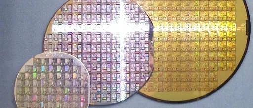
Often, we encounter the terms “tape-out” and “wafer” and many people mistakenly believe they refer to the same concept. In fact, the connotations and emphases of the two are completely different. In simple terms, tape-out is a process, while a wafer is a physical medium. Let’s break this down step by step. 1. Debunking Myths … Read more

The Rise of ‘Invisible Film’ in Chip Lithography: Japan and South Korea Dominate 80% of the Market, While Domestic Breakthroughs Are Just Beginning

The Rise of 'Invisible Film' in Chip Lithography: Japan and South Korea Dominate 80% of the Market, While Domestic Breakthroughs Are Just Beginning

In chip manufacturing workshops, there is a key material that is “invisible yet indispensable” — it acts like a high-precision “film” that accurately transfers chip design blueprints onto silicon wafers. Without it, even the most complex chip designs cannot be mass-produced. This material is the photomask, and its “core framework” — the blank mask — … Read more

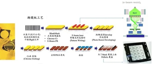
The Uses and Production Process of Reticles and Photomasks in Semiconductor Lithography Materials

The Uses and Production Process of Reticles and Photomasks in Semiconductor Lithography Materials

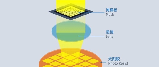
What is a Reticle (Photomask/Mask)? Reticles and photomasks are collectively referred to as PhotoMasks (including Reticle, Mask). •[Mask,Pellicle (protective film),DUV,ArF,I-line,EUV,reflective masks] Reticle is a photomask that contains the designed pattern in the lithography process. The detailed structure of the mask includes a Pellicle (thin polymer functional film) and a quartz glass plate, and it blocks … Read more

Photomasks: The Invisible Key to Chip Competition

Photomasks: The Invisible Key to Chip Competition

Photomask / PHOTOMASK Did you know? The billions of fine circuits on a chip rely on a “micro film” to accurately “draw” them out — this is the photomask. From 193nm deep ultraviolet to 13.5nm extreme ultraviolet, from 28nm mass production to 14nm breakthroughs, this “small slice” of quartz and chromium film hides the core … Read more

Chip Journey (5) – The Start of Tapeout and Costly Investments

Chip Journey (5) - The Start of Tapeout and Costly Investments

In the previous article “Chip Journey (4) – Introduction to Tapeout Design”, the design company and foundry have communicated the tapeout requirements through specified channels. This article begins to introduce the tapeout process for chips, which is also the start of another costly phase of the project.For the fab, the tapeout process generally includes the … Read more

An Overview of Semiconductor Materials: Analysis of Five Major Fields and Representative Companies

An Overview of Semiconductor Materials: Analysis of Five Major Fields and Representative Companies

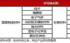
Semiconductor materials include wafer manufacturing materials and packaging materials. Wafer manufacturing materials include silicon wafers, mask plates, electronic gases, photoresists, CMP polishing materials, wet electronic chemicals, target materials, etc. Packaging materials include packaging substrates, lead frames, bonding wires, encapsulation materials, ceramic substrates, chip bonding materials, and other packaging materials. Table 1-1 Classification of Semiconductor Materials … Read more