 👆If you would like to meet regularly, feel free to star 🌟 and bookmark it~Source: This article is translated from semiengineering, thank you.
Intel’s foundry, TSMC, and Samsung Foundry are competing to provide all the essential components for complete 3D-ICs, which will achieve significant performance improvements with minimal power consumption in the coming years.
Much attention is focused on advancements in process nodes, but the successful implementation of 3D-ICs is far more complex than merely scaling digital logic. It requires new materials, different methods for handling thinner substrates and assembling them. It involves various back-powering schemes, different types of bridges, interface standards for multi-chip communication, and new interconnect technologies and methods. Additionally, it necessitates significant changes in EDA tools and methods, digital twins, multi-physics simulations, restructuring engineering teams and processes, and integrating AI at multiple stages throughout the design-to-manufacturing process.
3D-ICs have been on the internal roadmaps of foundries for over a decade, but it was only two years ago, with the launch of ChatGPT and the subsequent construction of AI data centers, that complete chip stacking truly gained momentum. Since then, the focus has been on significantly improving power consumption and performance, and the best way to achieve this is by decomposing SoCs, processing a large number of computational elements in parallel, and reducing the distance, resistance, and capacitance encountered when signals travel back and forth between different processing elements and memory.
Vertical Advantages
These goals are evident, but some of the technologies required to achieve them are still under development. For this reason, all foundries have announced plans to invest approximately $100 billion each over the next few years to achieve mass production of 3D-ICs. Many issues need to be resolved, most of which must be addressed in advance and validated on wafers before they can be realized. From a technical or economic perspective, relying solely on the advantages of planar scaling in terms of power consumption, performance, and area/cost is no longer sufficient.
Kevin Zhang, Senior Vice President of Business Development and Global Sales at TSMC, stated, “Transistor technology and advanced packaging integration must advance in tandem to provide our customers with complete product-level solutions. The combination of 3D structural technologies is very important to us.”
It is well known that signal transmission speeds within a planar system-on-chip (SoC) are faster than the signal transmission speeds between different chips in some system-level packages (SoCs). However, despite the continuous scaling of digital transistors, SRAM and interconnects cannot scale. At the most advanced nodes, packaging all components onto a single chip of photomask size often results in low yields and significantly reduces first silicon success rates.
To address this challenge, system companies and leading processor suppliers have begun to decompose SoCs and transform them into chipsets using advanced packaging. Smaller, functionally concentrated chipsets have higher yields than large SoCs, and the design costs for each chipset are lower. Moreover, theoretically, chipsets can be infinitely assembled into custom packages to enhance performance.
However, the performance of these multi-chip components can drop sharply when data needs to move back and forth between memory and processing elements. This is known as the memory wall, which relates to distance and the speed of signal transmission over wires. High Bandwidth Memory (HBM) is already good enough for L3 cache. It is much faster than standard DRAM due to its wider channels (HBM4 has 2,048 channels), which helps reduce resistance and capacitance. However, SRAM remains faster, making it the preferred memory for L1 and L2 caches. SRAM is typically configured with six transistors, which significantly improves access speed compared to DRAM, which uses one transistor and one capacitor. Capacitors are needed to address charge leakage issues, which can sometimes occur spontaneously when DRAM heats up.
Hybrid methods help, and stacking more layers of HBM is also effective. Samsung, SK Hynix, and Micron are among the few companies producing HBM. Samsung has used this as a springboard to begin customizing HBM for specific workloads. However, the best solution is a combination of HBM and SRAM, and the latest roadmaps from foundries showcase complex combinations of different memory types with very tight interconnect spacing to facilitate data movement.
Intel’s latest architecture shows that the 14A logic layer is directly stacked above the SRAM layer.
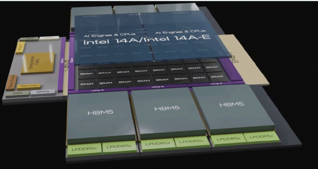
Figure 1: Intel’s 3D-IC concept, where the 14A chip is packaged above the SRAM and connected to I/O via EMIB bridging technology, surrounded by HBM for L3 cache.
“Everyone is talking about the memory wall,” said Kevin O’Buckley, Senior Vice President and General Manager of Intel Foundry. “As we continue to scale more and more cores and push for higher computing performance, ensuring the ‘beast’ runs smoothly is a top priority. 3D technology is one example that allows us to allocate a significant portion of the chip area to SRAM without sacrificing all the area to meet the still-required computing demands.”
However, this approach requires a completely different chip assembly method. Logic stacking technology has also been brewing for years but has been largely shelved due to thermal issues. Its goal is to double transistor density by adding another layer of processing elements and memory, allowing them to operate as a single system.
Taiwan Semiconductor Manufacturing Company (TSMC) Chairman Morris Chang stated, “We started with face-to-face integration, connecting two chips together. We are also developing face-to-face integration technology that allows customers to maximize interconnect density between two chips. If we stack chips together, you will find that the ultra-bonding spacing will continue to shrink from 9 microns to 6 microns, and then all the way down to 5 microns and below. This integration will adopt both face-to-face and face-to-face methods to meet different application needs.”
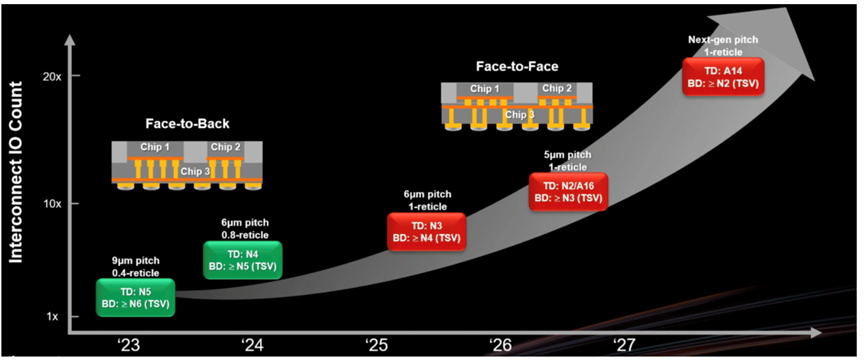
Figure 2: TSMC’s 3D IC roadmap showcasing different integration strategies.
In a presentation last spring, Taejoong Song, Vice President of Development at Samsung Foundry, showcased a roadmap featuring logic stacking technology (LCOE) that combines 2nm (SF2) chips with 4nm (SF4X) chips, both mounted on another substrate. This is essentially a 3D-IC on a 2.5D package (sometimes referred to as 3.5D). Song stated that the foundry will begin stacking SF1.4 on SF2P starting in 2027.
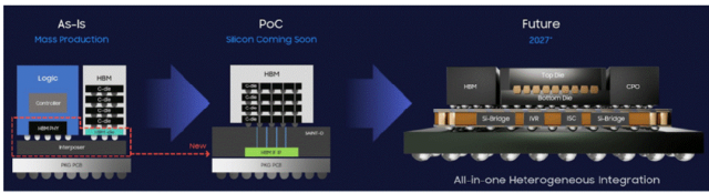
Figure 3: Samsung’s 3D IC roadmap.
Vertical Limitations
Regardless of the layout, heat dissipation remains the biggest challenge and the most common reason for the slow progress of 3D integrated circuits. Since then, the situation has changed significantly, and leading chip manufacturers need to work together to address the demands for performance and power.
While the specific delivery dates for this technology remain unclear, all three foundries currently prominently feature 3D-ICs on their roadmaps. This solution may involve combining logic developed at the latest nodes with N-1 or N-2. However, the goal is tighter integration, allowing them to operate as a single system and connect via high-speed interfaces to other critical components that have been stripped from planar SoCs.
In recent years, various solutions have emerged to eliminate residual heat, but not all solutions are ready for mass production. These include:
Thermal vias. Silicon vias can be used to conduct heat directly from processing elements to external heat sinks. The challenge here is determining the number and location of these “micro-chimneys,” as different workloads generate different thermal gradients.
Steam caps. This method works similarly to evaporative (also known as swamp) coolers. When gas flows through a wet pad, it absorbs liquid and then evaporates, transferring some heat to the external heat sink. Initial experiments with this method failed because the target device was a mobile phone, which constantly moves and vibrates. However, in data centers, server racks are fixed during use, making this method more feasible and relatively inexpensive.
Microfluidic technology. This concept dates back to the 1980s when mainframes required water cooling. (Some systems now offer optional water cooling again, but it is not mandatory.) This made upgrades difficult, and like all piping, leaks sometimes occur. After air-cooled small computers and racks filled with PC server blades were installed, many customers saw this as a significant advantage. However, as transistor density increases and workloads grow, the flow of liquid in tiny channels has once again become a subject of active research.
Thermal interface materials. These materials come in the form of pads, pastes, and solid materials (including recent carbon nanotubes) that conduct heat well but are expensive and relatively lacking in long-term testing. The industry is still working to determine the best materials and how to use them in combinations to achieve economies of scale.
Immersion. While it sounds counterintuitive, electronic devices can be immersed in inert liquids without causing short circuits. The challenges here are reusability, sustainability, and cost.
Data-Driven Design
The increase in the number of transistors in multi-chip components also exacerbates wiring congestion. Advanced layout and routing tools can achieve much of the automation, but they cannot solve all power delivery issues for all transistors, which is critical for maintaining performance. For this reason, all three foundries have developed or are developing back-power delivery (BPD) technologies:
Intel’s PowerVia BPD will be paired with RibbonFET nanosheet transistors in this year’s 18A node;
TSMC will launch Super Power Rail BPD with the A16 node in the second half of 2026;
Samsung will offer SF2Z BPD at the 2nm node starting in 2027.
Moving the power delivery network off-chip shortens the power delivery distance and simplifies signal transmission between the various metal layers within the chip. Therefore, routing no longer requires complex wiring but becomes simpler, especially between chips filled with silicon vias and connected through hybrid bonding.
Mick Posner, Senior Director of Cadence, stated, “You have the ability to install thousands of TSVs between chips. That’s great, but they each require 0.003 picojoules per bit, which is a very small number. However, when you cram them all into a 1 square millimeter space, it adds up. You need to perform hotspot analysis, manage power consumption, and other tasks for compute-intensive chips, which will be a challenge. Power density is already high, and we have seen thermal expansion lead to chip stack fractures. There are many challenges. But also consider the potential for performance improvement. Since width is limited, we must go up. So why not build a skyscraper?”
This is the basic idea. However, to fully leverage the advantages of chip stacking, these layers need to become thinner to shorten signal transmission distances. Moreover, not all layers need to be stacked. For example, HBM can be designed to surround the 3D-IC logic stack and connect with I/O and other memory at high speeds.
To truly accelerate speeds, some of these connections may adopt optical interfaces and co-packaged optical devices. All major foundries are incorporating co-packaged optical devices into their development plans, as light can transmit data at extremely high speeds while accumulating lower power consumption and heat.
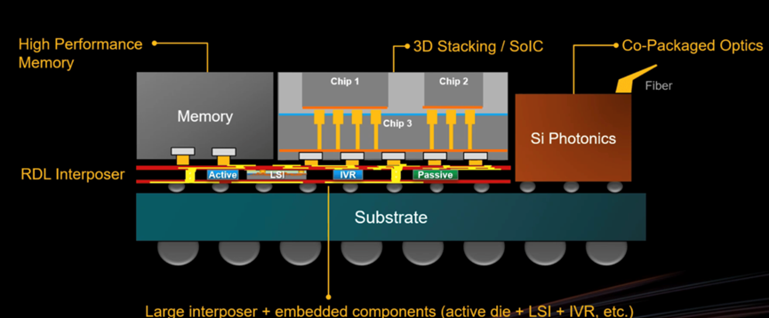
Figure 4: TSMC plans to integrate co-packaged optical devices with its 3D-IC model.
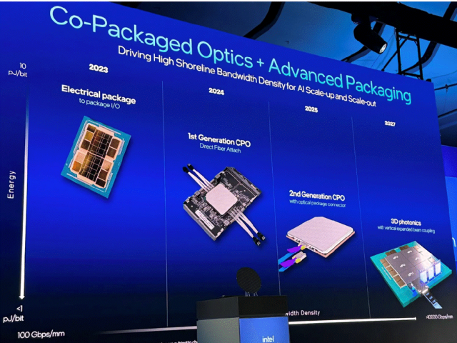
Figure 5: Intel’s optical roadmap.
Naga Chandrasekaran, Chief Technology and Operations Officer and General Manager of Intel’s chip foundry business, stated in a recent speech, “Optical interconnects have significant advantages over traditional electrical I/O. In terms of coastline density improvement, it has advantages in bandwidth, latency, and energy efficiency. When we can elevate optical interconnects to the chip-to-chip level and combine them with Intel’s advanced packaging capabilities, this solution will provide significant advantages in our expansion and scaling of AI-based solutions. It will offer denser and more advanced interconnect capabilities. Furthermore, in the computing domain, by adopting co-packaged optical solutions, we can provide lower latency and higher throughput.”
Like most issues in 3D-ICs, this is harder than it sounds. First, light does not bend around corners, so waveguides cannot have any right angles. They also need to be smooth, as any roughness will have the same effect as edge roughness in electrical interconnects. Additionally, light reacts to heat, and under unpredictable workloads, it may cause its offset to exceed expectations.
“Today, computing systems are not just contained on a single motherboard,” said Intel’s O’Buckley. “In most cases, it is not even in a rack. If you look at what some of the largest systems companies on Earth are doing today, such as hyperscale computing companies or the AI systems being developed by NVIDIA, you will find that connectivity is as important as computing power, and they can scale performance metrics. Copper cables have been the backbone of our industry for generations, while fiber optics are the links connecting towns. Now, fiber technology allows for terabit-level bandwidth to be consistently transmitted between racks, which is crucial. This connection used to be done at the switch level. But due to the demands for consistency and latency from these systems, we are now discussing directly connecting fiber to compute clusters instead of through switches. There is no doubt that this is the direction the industry is heading.”
At least part of the solution is smart placement of optical components. “It largely depends on the location of the laser source,” O’Buckley said. “Some innovations in the optical field today, such as multiplexing, are often less sensitive to temperature. You can place them close to the computing point. Then, for the laser source and some sensing devices, you can move them a bit further away. Arranging some optical components in this way allows you to decompose the laser to some extent, which is what some companies are choosing to do.”
TSMC’s Zhang Yong stated that photonic technology can also be used to reduce chip heat. “In the near future, we will see customers using integrated silicon photonic technology to transmit signals and achieve interconnections between chips. We all know that in terms of signal transmission, photons are far more efficient than electrons. Electrons excel in computation, but photons outperform in signal transmission.”
Zhang noted that another key option is integrated voltage regulators, which will further enhance power efficiency. “This is very important because customers or future AI products want to integrate multiple logic circuits and multiple HBM together. These circuits will consume a lot of power. Look at today’s advanced AI accelerators, which can consume up to 1000 watts. In the future, power consumption will reach several kilowatts. Integrating power supplies into such packages is very challenging, so integrated voltage regulators can reduce current demands because the number of pins is limited. You cannot directly input that much current.”
This, in turn, reduces the overall heat within the package.
Process Scaling
This may sound counterintuitive, but to maximize the performance advantages of 3D-ICs, continuous process scaling is required. The reason is not the performance of transistors—though chip manufacturers can certainly take full advantage of that—but rather dynamic power density. Smaller transistors are more energy-efficient, helping to reduce heat and lower energy costs in large data centers. Additionally, the transition from FinFETs to Gate-All-Around FETs reduces static leakage, which also generates heat that can become trapped in the package.
Take TSMC’s upcoming A14 node as an example, which is the next full node after 2nm for the foundry. Zhang noted, “The scaling advantages of A14 compared to our previous generation are very significant. It has a speed improvement of up to 15%, a power reduction of 30%, and a logic density increase of 1.23 times. Overall chip density has increased by at least 1.2 times, so this is a very, very effective technology. This technology also employs NanoFlex Pro technology. This is actually the result of design technology co-optimization, allowing designers to design products in a very flexible way to achieve optimal power and performance advantages. This technology will go into production in 2028.”
Zhang pointed out that the first version of this node will not include back-power delivery until the second version of A14 in 2029.
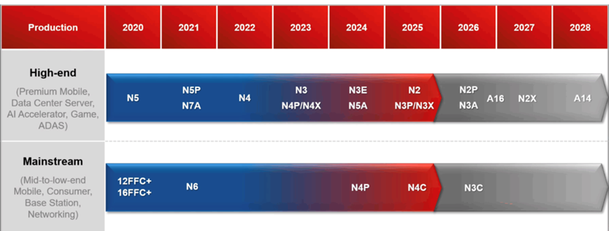
Figure 6: TSMC’s process roadmap.
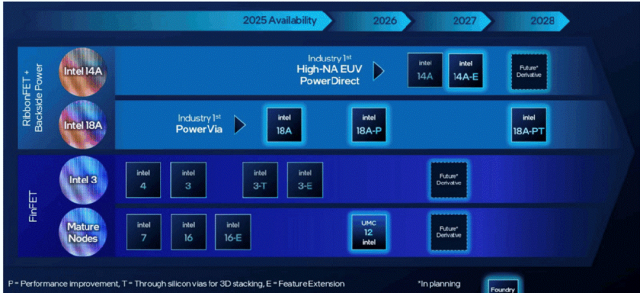
Figure 7: Intel’s process roadmap.
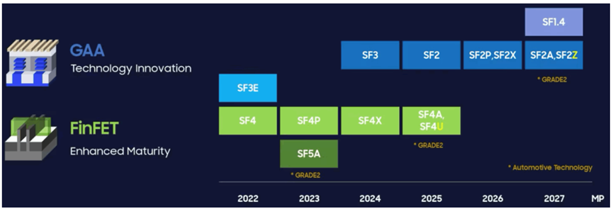
Figure 8: Samsung’s process roadmap.
Of course, scaling down still presents some common issues. Thinner dielectrics may fail faster, leading to crosstalk and other potential signal interference. Thinner chips in 3D-IC stacks also face the same issues, losing the insulating properties of thicker substrates and accelerating TDDB. These issues will significantly impact the industry’s design and assembly methods for these devices, making routing more complex and requiring more simulation, verification, and debugging work.
Sassine Ghazi, President and CEO of Synopsys, stated in a recent speech, “3D-IC is the only way to scale the number of transistors to hundreds of billions or even trillions. But once you start scaling to this level of complexity, the only way to achieve performance or power goals is to improve the efficiency of the interconnect layers and build multi-die systems efficiently. The dies may come from different process technologies or even different foundries. You must verify and confirm the architecture to deliver this advanced packaging.”
Future Applications
The initial applications of 3D-ICs will focus on AI data centers, but once the processes are refined and issues resolved, this approach will be able to be applied more broadly and achieve more targeted component combinations. Whether all applications require complete 3D-ICs or only some core technologies remains to be determined. Nevertheless, the technical issues being addressed in stacked chips will have broad application prospects.
“We believe there is a huge space for mobile innovation,” said TSMC’s Zhang Yong. “We believe one device that can drive business growth in the future is augmented reality glasses. These glasses are transparent, compact, and can be worn all day. To achieve all-day battery life and powerful computing capabilities, you really need advanced chips. You need a lot of sensing devices. You need connectivity, so you need a lot of chips.”
He also mentioned humanoid robots. “The automotive industry wants to achieve autonomous driving. You can think of a car as just the first step in making a robot. A car is a simple robot that just takes you from point A to point B. But in the future, if you really want a robot that can interact with humans, help you with daily chores, and even handle many things that humans do not want to do, you need to create these so-called humanoid robots. If you look inside these robots, you will see a lot of chips. First, you need to have intelligence. You need to have good AI capabilities. You need advanced chips to drive that intelligence. You also need good sensing capabilities and strong power output. You need a lot of integrated controllers to provide the ability to operate under different conditions.”
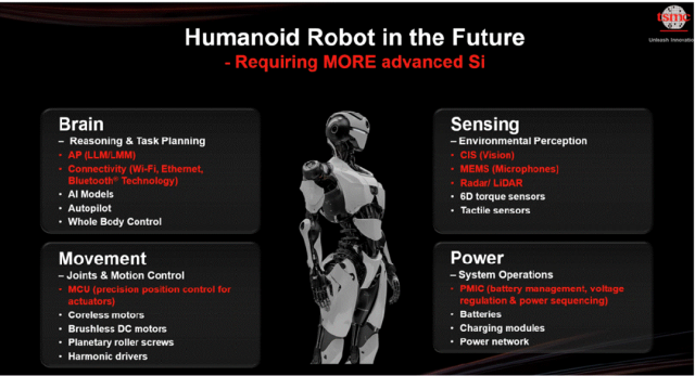
Figure 9: Chip requirements for humanoid robots.
Conclusion
Different foundries are at different stages in developing all the necessary components for 3D-ICs. No single foundry can solve all these problems at once, and the inclusiveness of the chip industry has increased today. With ongoing geopolitical disruptions in the supply chain, chip manufacturers are looking for multiple sources and various technology options.
Mike Ellow, CEO of Siemens EDA, stated, “We are facing challenges, opportunities, and dilemmas at the same time. How can we guide early engineers and professional engineers to enable them to complete the many new designs that must be delivered and have the required chips? The world relies on a resilient, robust, distributed advanced node chip supply chain. Beyond that, we also need a set of technologies that integrate AI to connect a broader ecosystem to support the creation of all design content.”
Original Link
https://semiengineering.com/three-way-race-to-3d-ics/
END
👇 Recommended Semiconductor Quality Public Account 👇
▲ Click the card above to follow
Focusing on more original content in the semiconductor field
▲ Click the card above to follow
Follow global semiconductor industry trends and developments
*Disclaimer: This article is original by the author. The content of the article reflects the author’s personal views, and Semiconductor Industry Observation reprints it only to convey a different perspective, which does not represent Semiconductor Industry Observation’s endorsement or support of this view. If there are any objections, please contact Semiconductor Industry Observation.

This is the 4025th issue shared by “Semiconductor Industry Observation” for you, welcome to follow.
Recommended Reading
★A Chip That Changed the World
★U.S. Secretary of Commerce: Huawei’s Chips Are Not That Advanced
★“ASML’s New Lithography Machine, Too Expensive!”
★The Quiet Rise of NVIDIA’s New Competitors
★Chip Crash, All Blame Trump
★New Solutions Announced to Replace EUV Lithography!
★Semiconductor Equipment Giants, Salaries Soar by 40%
★Foreign Media: The U.S. Will Propose Banning Software and Hardware Made in China for Cars


『The First Vertical Media in Semiconductors』
Real-time, Professional, Original, In-depth
Public Account ID: icbank
If you like our content, please click“Looking” and share it with your friends!