On the 27th, reporters learned from West Lake University that West Lake Instruments (Hangzhou) Technology Co., Ltd. (hereinafter referred to as “West Lake Instruments”), incubated by the university, has successfully developed an automated laser peeling technology for 12-inch silicon carbide substrates, solving the challenges of slicing ultra-large silicon carbide substrates of 12 inches and above.
Compared to traditional silicon materials, silicon carbide has a wider bandgap, higher melting point, electron mobility, and thermal conductivity, allowing it to operate stably under high temperature and high voltage conditions. It has become a key material for the iterative upgrade of the new energy and semiconductor industries.
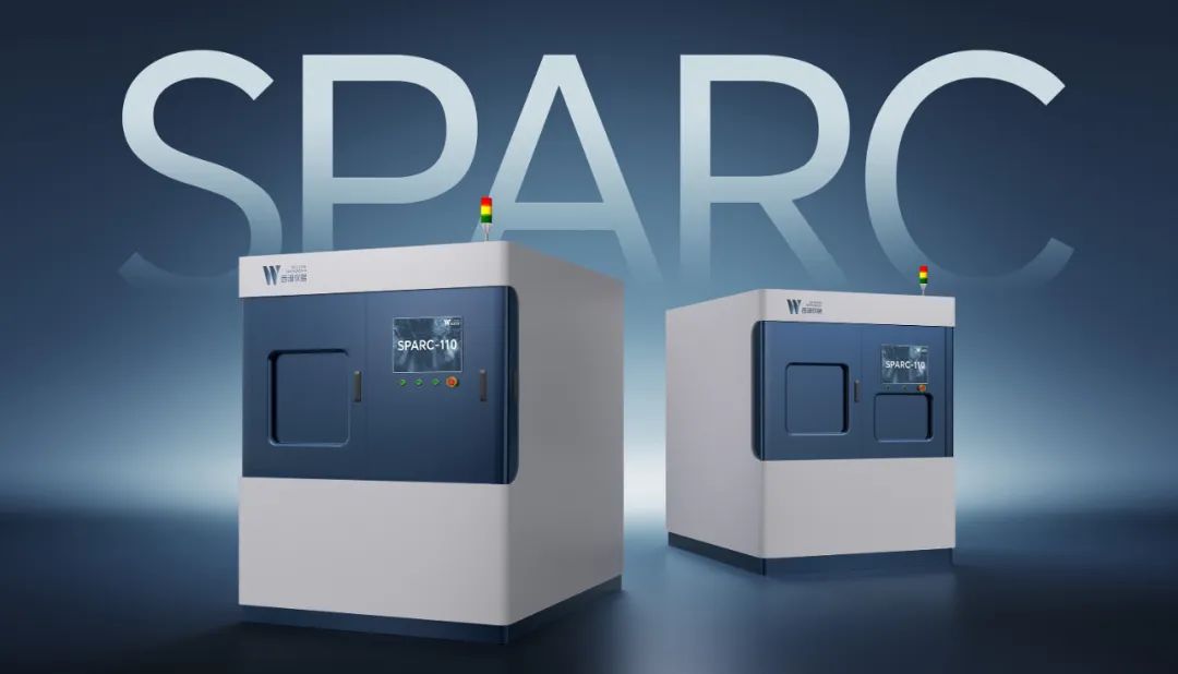
▲Silicon carbide substrate laser peeling system. Image source: West Lake University
“Currently, the cost of silicon carbide substrate materials remains high, severely hindering the large-scale application of silicon carbide devices.” Professor Qiu Min from the School of Engineering at West Lake University explained that one of the important ways to reduce costs and increase efficiency in the silicon carbide industry is to manufacture larger-sized silicon carbide substrate materials. Compared to 6-inch and 8-inch substrates, the 12-inch silicon carbide substrate material expands the area available for chip manufacturing on a single wafer, significantly increasing chip yield and reducing the unit manufacturing cost of chips under the same production conditions.
According to predictions from international authoritative research institutions, the global silicon carbide power device market size will reach $6.7 billion by 2027, with a compound annual growth rate of 33.5%. At the end of last year, domestic companies disclosed the latest generation of 12-inch silicon carbide substrates. The demand for ultra-large silicon carbide substrate slices of 12 inches and above has emerged.
Previously, West Lake Instruments had already launched 8-inch conductive silicon carbide substrate laser peeling equipment. In response to the latest market demand, West Lake Instruments quickly introduced ultra-large silicon carbide substrate laser peeling technology, applying ultra-fast laser processing technology to the silicon carbide substrate processing industry, completing the development of related equipment and integrated systems.
“This technology has achieved automation of the processes of thinning silicon carbide ingots, laser processing, and substrate peeling.” Qiu Min explained that compared to traditional cutting technologies, the laser peeling process has no material loss, significantly reducing raw material waste.
Qiu Min stated that the new technology can greatly shorten the substrate slicing time, making it suitable for the future large-scale production of ultra-large silicon carbide substrates, further promoting cost reduction and efficiency improvement in the industry.