Author | Du Wenjing, Chang Liang
The AIGC led by large models marks the starting point of the Fourth Industrial Revolution, possessing the ability to fundamentally change the rules across various industries. The year 2023 has become the inaugural year for AI large models, with significant improvements in pre-training and generative capabilities, as well as multimodal and multi-scenario application capabilities. Among these, computing power chips, as the most important productivity tool, have become the focus of global technological competition.
In recent years, the United States has frequently introduced sanctions against China’s semiconductor industry, attempting to curb China’s rise in the chip sector. However, this series of sanctions has not only failed to hinder the development of China’s semiconductor industry but has also stimulated China’s determination and motivation for independent innovation in chip technology. In this context, advanced packaging technology, which can effectively enhance chip performance, has gradually become a key breakthrough for domestic AI chips to achieve a leapfrog development.
01
Post-Moore Era,
Advanced Packaging is Inevitable
The main purpose of semiconductor packaging is to provide electrical connections and protect the chip. Advanced packaging technology is primarily distinguished from traditional packaging technology by whether it uses wire bonding. Traditional packaging generally utilizes lead frames as carriers and employs wire bonding for interconnection. In contrast, advanced packaging uses pin arrays for electrical connections and employs flip-chip bonding and other interconnection methods, leading to the development of various packaging technologies.
The differences in packaging technology directly affect the chip’s performance, power consumption, and size. Therefore, packaging plays a crucial role in determining the overall functionality of electronic devices. With the growing demand for smaller, faster, and higher-performance chips, advanced packaging technology has become particularly important.
In the “post-Moore era,” as integrated circuit processes become increasingly advanced, significant challenges arise on both the technical and cost fronts, leading to rapid development in advanced packaging.
Advanced packaging has extended various solutions based on different needs, aligning with the characteristics of different scenarios, including flip-chip packaging, wafer-level packaging, system-level packaging, and 2.5D/3D packaging, primarily achieving densification of connections, diversification of stacking, and systematization of functions through innovations in planar and spatial designs. With the evolution of new technologies, advanced packaging processes represented by 2.5D/3D have deeply penetrated the production of high-performance AI chips.
In the 2.5D/3D advanced packaging process, key elements such as Bump, RDL, Interposer, and TSV are involved, all of which relate to processes with characteristics of front-end processes. Compared to traditional packaging, these have higher technical thresholds and entry barriers. Therefore, after entering the advanced packaging era, the global competition landscape in packaging and testing has changed, with advanced packaging markets no longer limited to packaging players; wafer fabs are also participating and developing rapidly.
Taking TSMC as an example, 3D Fabric is TSMC’s advanced packaging technology brand, encompassing various 2.5D and 3D packaging technologies. Among them, the CoWoS platform integrates advanced logic and high-bandwidth memory (HBM), widely used in artificial intelligence, machine learning, and data centers.
CoWoS (Chip On Wafer On Substrate) technology is an important technology platform for TSMC in 2.5D packaging. CoWoS is derived from the combination of CoW and oS: using micro-bump (μBumps) technology, the chip is first connected to the silicon wafer (Si interposer) through the Chip on Wafer (CoW) packaging process, and then the CoW chip is connected to the substrate, forming CoWoS.
In this process, the silicon interposer first forms through TSV technology to create through-silicon vias, and then RDL is used to form high-density wiring, allowing signals to be transmitted at high speeds through the silicon interposer. CoWoS is particularly suitable for applications requiring a large amount of parallel processing, handling large data vectors, and needing high memory bandwidth.
Illustration of TSMC’s CoWoS packaging structure
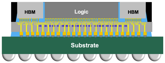
Source: TSMC official website
TSMC’s CoWoS technology is a leading technology in 2.5D packaging, and related technical solutions have become a major direction for learning in the industry. Samsung and Intel have also prioritized advanced packaging technology as a development focus, both having completed deployments of 2.5D/3D packaging. Samsung’s I-Cube, as a heterogeneous integration technology, can integrate one or more logic chips (such as CPU, GPU, etc.) and multiple memory chips (such as HBM) on top of the interposer. Intel has introduced EMIB (Embedded Multi-Die Interconnect Bridge) technology in 2.5D packaging, which structurally does not introduce an additional silicon interposer but instead adds a silicon bridge layer at the edge connection of two bare chips, customizing the I/O pins at the edges of the bare chips to match the bridging standards.
Nevertheless, CoWoS currently remains the most mainstream packaging solution for AI computing power chips, widely adopted by companies such as NVIDIA, Broadcom, Marvell, Google, Amazon, and AMD, with NVIDIA accounting for more than half of the demand. TrendForce predicts that TSMC’s total CoWoS capacity will increase by 150% in 2024, reaching a monthly capacity of nearly 40,000 pieces by the end of 2025, and is expected to reach 90,000 to 110,000 pieces per month by 2026.
According to Yole’s forecast, the share of advanced packaging in the overall packaging industry will increase from 47% in 2022 to 58% in 2028; it is expected that by 2029, the market size of advanced packaging will reach $69.5 billion, with a CAGR of over 10% from 2023 to 2029. Among them, the demand for AI computing power will drive significant growth in 2.5D/3D packaging, with the market size expected to reach $27.6 billion by 2029, making it the largest and fastest-growing market segment within advanced packaging.
02
Advanced Packaging:
The Breakthrough Point for Domestic AI Chips
Since the outbreak of the China-US trade war in 2018, the US’s blockade of China’s chip technology has gradually evolved from targeting individual companies to suppressing the entire industry chain.
In December 2020, the US placed SMIC on the “Entity List,” restricting SMIC’s expansion of 14nm and below processes, limiting domestic advanced process foundry capabilities.
In October 2022, the US issued new regulations on export controls for advanced computing and semiconductor manufacturing, implementing a “trinity” of technical restrictions through blocking advanced semiconductor equipment, cutting off supplies of high-end computing chips from NVIDIA, and obstructing talent flow, causing structural shocks to China’s semiconductor industry, which continue to escalate.
In November 2024, under US pressure, TSMC plans to stop supplying chips with 7nm and more advanced processes to mainland China, affecting AI chips that meet any of the following conditions: (1) chip area of 300mm² or more; (2) using high-bandwidth memory (HBM) or 2.5D packaging CoWoS technology; (3) transistor count exceeding 30 billion. This policy aims to further curb the production and manufacturing of domestic AI chips from the upstream foundry and packaging segments.
On January 15, 2025, the US Department of Commerce’s Bureau of Industry and Security (BIS) announced revisions to export control regulations (EAR), requiring more due diligence procedures related to advanced computing integrated circuits. A chip that uses advanced processes at the 16/14nm node or below and contains 30 billion or more transistors in its final packaging will be restricted, and relevant front-end chip manufacturers and OSAT companies will be prohibited from exporting such chips to China.
By 2027, the transistor count will expand to within 35 billion; by 2029 or later, it will further expand to within 40 billion. TSMC also announced that starting January 31, 2025, if products related to 16/14nm processes are not packaged by an “approved OSAT” on the BIS whitelist, and TSMC has not received a certified signed copy from that packaging factory, these products will be suspended from shipment.
This series of sanctions has significantly increased the difficulty for Chinese companies to obtain and manufacture high-end AI chips, but it has also accelerated China’s progress in independent research and domestic substitution, with advanced packaging expected to become a technological breakthrough point:
(1)Breaking Process Limitations
The restrictions on high-end lithography machines have led domestic foundries to face technical bottlenecks in advanced process chip manufacturing. Multi-die integration technology based on advanced packaging can enhance chip performance and break through the blockade of US advanced processes. Generally, the more transistors per unit area, the stronger the chip performance. Advanced packaging technology can integrate multiple small chips together through integration processes, helping chips leap across 1 to 2 process nodes, enhancing overall system performance;
(2)Optimizing Heterogeneous Computing
Advanced packaging can also achieve system-level packaging of computing modules with different process nodes, such as logic chips, memory units, and analog circuits, significantly improving energy efficiency;
(3)Breaking Interconnection Bottlenecks
By using silicon-based interposers or hybrid bonding technologies, the interconnection bandwidth between chips can be increased by 1-2 orders of magnitude, alleviating the constraints of the “memory wall” on computing power.
The combined application of these technological paths can shift the competition for domestic AI chips from a single process metric to a multidimensional competition of “architectural innovation + heterogeneous integration + system optimization,” providing domestic AI chips with the opportunity to leverage a vast market application landscape and rapidly iterating engineering capabilities to significantly narrow the technological gap and break through technical bottlenecks.
03
The Development Status and Prospects of the Domestic Advanced Packaging Industry
In recent years, China has made significant progress in advanced packaging technology, with leading domestic packaging and testing companies actively laying out their strategies. Changdian Technology has launched the XDFOI high-density fan-out packaging solution for Chiplet heterogeneous integration applications. Tongfu Microelectronics has introduced an advanced packaging platform, VISionS, which integrates 2.5D, 3D, and MCM-Chiplet technologies. Huada Semiconductor has a 3D Matrix platform based on fan-out packaging technology, with certain TSV capabilities, mainly applied in 5G communications, medical, and IoT fields.
Additionally, a number of growing enterprises have emerged in the domestic market, actively entering the advanced packaging field, but the high-end advanced packaging sectors such as 2.5D/3D remain blue ocean markets, presenting development opportunities for new entrants.
At the same time, the industry chain has also raised higher requirements for high-end advanced packaging and testing segments.
First, advanced packaging factories need to deeply build design service capabilities. With the popularization of heterogeneous integration and system-level packaging technologies, the synergy between packaging design and front-end chip design has become crucial. Packaging factories with the ability to independently develop EDA tools, multi-physical field simulation platforms, and system architecture optimization experience can intervene from the product definition stage, providing customized design services such as signal integrity analysis, thermodynamic simulation, and power consumption optimization.
For example, for 2.5D packaging with HBM high-bandwidth memory chips, high-density interconnection design needs to be achieved through wiring optimization on the silicon interposer; in heterogeneous integration of Chiplets, advanced packaging design must address interconnections between bare chips of different process nodes and electromagnetic compatibility issues. This “design-process collaborative optimization” capability allows packaging factories to upgrade from mere foundry service providers to system-level solution providers.
Secondly, in the future, domestic wafer processes will form a Chinese route and Chinese nodes, which requires packaging factories to fully understand and connect with the front-end wafer fab processes, targeting key issues left over from the front-end, such as mechanics and thermal management, for targeted optimization, enabling precise control in material selection, process window setting, and defect analysis. Moreover, the processes involved in advanced packaging, such as Bump, RDL, Interposer, and TSV, all relate to front-end processes. Therefore, a deep understanding of front-end wafer manufacturing processes will become the technical foundation for advanced packaging.
At the same time, as the demand for computing power shows exponential growth, a single packaging technology can no longer meet the differentiated scenario needs from mobile terminals to supercomputing centers; a complete process platform can meet the multidimensional transformation of the semiconductor industry.
For instance, in the field of three-dimensional integration, it is necessary to master core technologies such as TSV deep hole etching (depth-to-width ratio >10:1), hybrid bonding, and ultra-thin wafer processing; in the planar expansion direction, breakthroughs in 2μm line width RDL re-routing and warpage control are required for high-density fan-out processes; and capabilities for co-packaging of optoelectronics (CPO) and other heterogeneous integration are also needed. This platform-based architecture enables packaging manufacturers to flexibly iterate technology routes and quickly respond to market demands, forming a technological moat.
Therefore, companies with design service capabilities, a thorough understanding of wafer fab processes, and a complete process platform will be more competitive.
In summary, US chip sanctions have become a catalyst for advancing China’s semiconductor technology, with advanced packaging playing an increasingly critical role. Although these sanctions have posed numerous challenges, they have also accelerated China’s independent innovation and breakthroughs in packaging technology. This has profound strategic significance for enhancing national technological autonomy and addressing future technological challenges. Under the synergistic effects of policy guidance, market drive, and technological innovation, advanced packaging is expected to become the core engine for domestic AI chips to leapfrog development, providing a strategic pivot for domestic AI chips to cross the process gap.
>End>>> This article is reproduced from “JIC Investment Observation,” with the original title “Industry | US Chip Sanctions Escalate, Advanced Packaging Becomes the Next Strategic Pivot for Domestic AI Chips.”To share cutting-edge information and valuable insights, the Space and Network WeChat public account reprints this article, with edits.If not reproduced and cited according to regulations, we reserve the right to pursue corresponding responsibilities.Some images could not be traced to their original sources, so they are not marked in the text. If your rights are infringed, please contact us immediately.HISTORY/Previous Recommendations
Commercial rockets, it’s not easy to say I love you—(1) The aborted journey of commercial rockets
Commercial rockets, it’s not easy to say I love you—(2) The unreplicable SpaceX
Commercial rockets, it’s not easy to say I love you—(3) What is the future path of China’s commercial rockets?
>>>
In a passionate new era,
In a challenging new domain,
With the vigorous leaders,
Exceptional entrepreneurs,
Let’s explore together,
Experience together,
Perceive together,
Build better quality together,
Achieve higher value together,
Witness greater leaps in commercial space together!
—— “Space and Network,” observing, recording, disseminating, and leading.
>>>
· Founder of “Satellite and Network”:Liu Yufei
·Vice President of “Satellite and Network”:Wang Junfeng
· Team of WeChat public account (ID: satnetdy)Editors:Yan Ling, Ha Mei, Zhou Yong, Qiu Li, Huang Rong, Na NaLead reporters:Li Gang, Wei Xing, Zhang Xuesong, Huo Jian, Le Yu, Daozi, Zhao DongPlanning Department:Yang Yan, Ruo Yi, Li ZhenziVisual Director:Dong YanProfessional Photography:Feng Xiaojing, Song WeiDesign Department:Gu Meng, Pan Xihong, Yang XiaomingAdministrative Department:Jiang He, Lin ZiBusiness Department:Wang Jinxin, Jin YiFor original article reprint authorization, infringement of reprinted articles, submissions, etc., please add WeChat: 15910858067For business cooperation; exhibition design, corporate VI/CI and interior design, corporate culture construction and brand promotion; corporate reputation communication and overall marketing communication, please add WeChat: 13811260603For magazine subscriptions, please add WeChat:wangxiaoyu9960· Satellite and Network Branches:Chengdu Branch Head: Shen HuaiChangsha Branch Head: Bin HongpuXian Branch Head: Guo ZhaohuiQingdao Branch Head: Jiang Wei· Head of “Satellite and Network” Headquarters:Nong Yan· Conference and Event DepartmentHeads:Qiao Haoyi, Xu Kexin, Dong Jinfeng· Cooperation in investment and strategic levels:Liu Yufei· This platform’s contracted design company:Yihua Kaitian (Beijing) Cultural Creative Design Co., Ltd.· Head of Aerospace Plus (Shenzhen) Equity Investment Fund Management:Yang Yan