
Abstract
In recent years, the impact of humidity on the thermal characteristics of power devices has become a hot topic. However, the effect of humidity on the thermal resistance of power device chip solder has not been experimentally verified, and the mechanism remains unclear. This paper proposes, for the first time, the mechanism by which humidity affects the thermal resistance of power device chip solder based on experimental testing, case studies, and simulation models. The results indicate that humidity can invade the device and affect the transient thermal resistance in two aspects: ① chip solder; ② contact thermal resistance at the device shell surface. Furthermore, the effects of humidity on the thermal capacity, density, and thermal conductivity of chip solder are explored. The case studies show that if the water vapor content accounts for 0.1% of the total material in the chip solder layer, the thermal capacity, density, and thermal conductivity of the chip solder will change to 101.9%, 100.0135%, and 91.4% of their original values, respectively. The calibrated simulation model of thermal characteristics indicates that the increase in thermal capacity of the solder layer will lead to a decrease in the thermal resistance of the solder layer (with overall thermal resistance unchanged), while the decrease in thermal conductivity of the solder layer will cause an increase in the overall thermal resistance of the device. These two factors together affect the operational lifespan of power devices under actual outdoor application conditions.
0 Introduction
Power semiconductor devices such as Insulated Gate Bipolar Transistors (IGBTs) and Silicon Carbide Metal-Oxide-Semiconductor Field-Effect Transistors (SiC MOSFETs) are widely used in outdoor conditions such as offshore wind power, photovoltaics, and electric vehicles. Their operational reliability is influenced by a combination of environmental factors including temperature, humidity, and salt mist, which has garnered significant attention in recent years.
Currently, common humidity reliability tests include High Humidity High Temperature Reverse Bias (H3TRB), High Voltage-High Humidity High Temperature Reverse Bias (HV-H3TRB), and High Accelerated Stress Test (HAST), aimed at assessing the insulation performance of chips and the hermeticity of packaging. However, in practical applications, intermittent conduction of large currents in devices leads to fluctuations in chip junction temperature and corresponding thermal stress. Changes in temperature cause fluctuations in relative humidity, which in turn alters the thermal characteristic parameters of the device and leads to moisture absorption and expansion of packaging materials such as bond wires and chip solder. This process involves the coupling of thermal, moisture, and multi-physical fields. However, it remains unclear whether relative humidity affects the reliability of device packaging, and this uncertainty poses challenges for reliability assessment in practical engineering applications.
Wang Yanhao, F. Hoffmann, F. Wuest, and others have conducted power cycling tests (PCT) to assess packaging reliability and indirect coupling tests to evaluate the impact of humidity on packaging through high temperature and high humidity storage or high temperature and high humidity high voltage reverse bias. They found interactions between the two reliability tests. Literature [10] found that after 3600 hours of dual 85 environmental storage, carbon, oxygen, and silicon elements in the epoxy molding compound (EMC) packaging migrated to the bond wires, depositing at the bond wire feet and bond body, leading to corresponding corrosion and a decrease in aluminum content, which in turn shortened the power cycling lifespan of the device by several tens of times, exhibiting early failure characteristics. Literature [11] allowed the devices under test (DUTs) to operate under 85°C/85% relative humidity (RH) and 80% rated voltage (VCES) during HV-H3TRB testing for 2139 to 2429 hours until all devices reached the failure criteria for blocking leakage current (ICES), after which they were removed for power cycling tests until the saturation voltage drop (VCEsat) or junction-to-case thermal resistance (Rthjc) reached the failure criteria. Comparing their lifespan with that of devices undergoing only power cycling tests, the results indicated that the lifespan of devices aged under HV-H3TRB decreased, with the Weibull distribution median lifespan being about 80% of that of devices undergoing only power cycling tests. The fundamental reason is that the junction-to-case thermal resistance (Rthjc) of the DUTs increased early in the power cycling, leading to an increase in the maximum junction temperature (Tjmax). Due to the mismatch in the coefficient of thermal expansion (CTE) between materials, greater stress was generated, accelerating the aging process and shortening the power cycling lifespan. Moreover, the phenomenon of increased junction-to-case thermal resistance early in power cycling aging was preliminarily verified through transient thermal impedance (Zth).
Literature [12] conducted power cycling tests with environmental temperature and humidity, finding that compared to conventional power cycling, the power cycling lifespan under normal temperature and high humidity was shortened by about 13.6%. The fundamental reasons are: ① changes in thermal interface materials (TIM) due to moisture absorption, where the originally applied thermal grease position is occupied by water vapor, leading to an increase in contact thermal resistance at the shell surface; ② moisture absorption by shell materials increases thermal expansion stress during power cycling, accelerating the growth of cracks in the solder layer. Both factors work together to shorten the power cycling lifespan. In summary, the impact of humidity on the power cycling lifespan of devices includes corrosion, increased thermal resistance, and accelerated crack growth. Literature [11-12] both mention the impact of humidity on thermal resistance; however, the mechanism by which humidity affects device thermal resistance remains unclear. Considering that key indicators such as device operational reliability and lifespan in practical engineering applications are influenced by environmental temperature and humidity, this issue urgently needs to be addressed.
This paper aims to explore the mechanism by which humidity affects the thermal resistance of power device solder, reflecting the transient thermal impedance of device thermal characteristics. Three different packaging types of devices underwent 722 hours of high temperature and high humidity storage and thermal resistance testing. Based on material science and mass transfer theory, the process of humidity invasion is analyzed, and conclusions are drawn in conjunction with case studies and simulation analysis. First, this paper introduces the information of the devices under test, the basic principles of transient thermal impedance testing, the testing platform, and the process. Secondly, based on the testing results of the transient thermal impedance curves, the theory of humidity invasion is analyzed in depth, exploring the moisture absorption capacity of different materials and its impact on thermal resistance. Finally, a finite element simulation model of the relevant devices under test is established and calibrated, providing case studies in conjunction with material thermal characteristic parameters, and identifying the key mechanisms by which humidity affects the thermal capacity, density, and thermal conductivity of solder and their representation in the transient thermal impedance of the device junction-to-heat sink.
1 Testing Principles and Scheme
1.1 Information of Devices Under Test
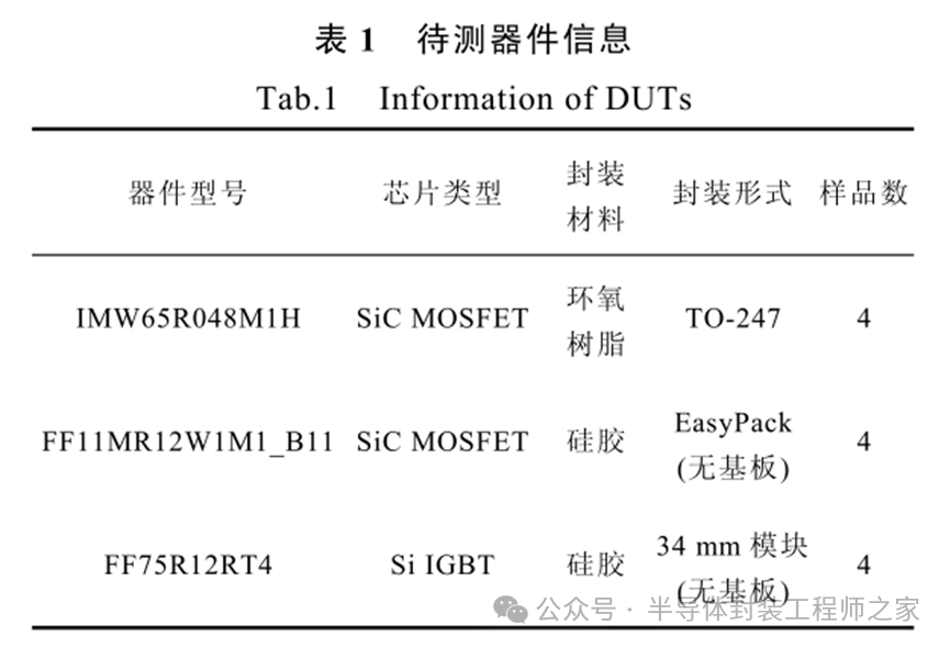
The devices under test (DUTs) are divided into three groups based on packaging type: TO-247 devices, EasyPack modules, and 34 mm modules, where the EasyPack module has no substrate, and the 34 mm module has a substrate. The TO-247 devices and EasyPack modules only have a chip solder layer, while the 34 mm module also has a system solder layer to characterize the moisture absorption capacity at different locations. The three groups of DUTs cover all existing soldered power device packaging structures on the market, making them typical and representative. The TO-247 devices and EasyPack modules use SiC MOSFETs, while the 34 mm module uses Si IGBT. Furthermore, each group is set with four DUTs to reduce random errors. The schematic cross-sectional structure of the three different packaging types of devices is shown in Figure 1, and the information of each DUT is listed in Table 1.
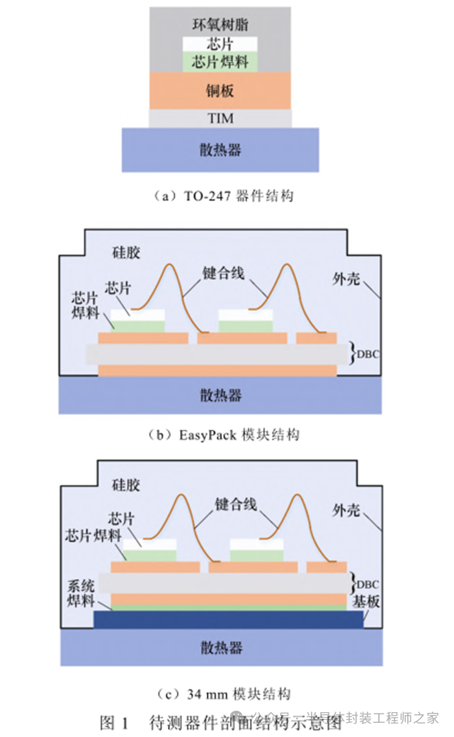
This experimental design aims to test the impact of humidity on the thermal resistance of device chip solder and characterize it through the junction-to-heat sink transient thermal impedance. Considering that thermal interface materials also exhibit moisture absorption behavior [12], the EasyPack and 34 mm modules are directly mounted on copper substrates to avoid the influence of moisture absorption from TIM materials such as thermal grease. The TO-247 devices, due to their copper base with no internal insulation, use Al2O3 ceramic sheets, which have poor moisture absorption but good thermal conductivity and insulation properties, as TIM for insulation and heat conduction.
1.2 Transient Thermal Impedance Testing
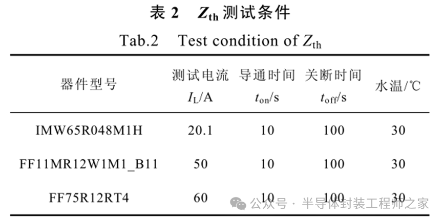
Transient thermal impedance characterizes the resistance encountered by heat as it transfers from the chip PN junction to the external heat sink, and is a key thermal characteristic variable that changes over time, effectively representing the thermal resistance and thermal capacity information of each material layer within the device packaging. The testing conditions for the transient thermal impedance Zth of the three groups of DUTs are shown in Table 2, with the test current set to maximize the junction temperature (Maximum Junction Temperature, MJT) as high as possible, close to the maximum allowable junction temperature (but still below it), to increase the signal-to-noise ratio of the measurement.
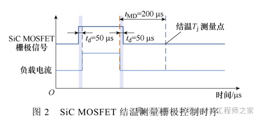
The calculation of transient thermal impedance is shown in Equation (1), where the key to testing is the accurate measurement of junction temperature during the cooling process [13]. For Si IGBTs, the saturation voltage drop method VCE(T) is generally used under small currents, while for SiC MOSFETs, the PN voltage drop VSD(T) of the body diode is used to achieve this, resulting in certain differences in the testing circuit [14]. For the junction-to-heat sink transient thermal impedance Zthjs of Si IGBT devices, the gate is fully turned on during testing, while for SiC MOSFET devices, the gate must be controlled to turn on the load current, and the gate must be turned off to allow the measurement current to flow entirely through the body diode (forward heating to measure junction temperature), using VSD(T) to measure junction temperature [14-15]. The gate control timing for SiC MOSFETs is shown in Figure 2, where the gate signal for the DUT is delayed by 50 μs compared to the load current falling edge, and the maximum junction temperature Tjmax measurement point is set with a 200 μs delay to ensure accurate measurement.
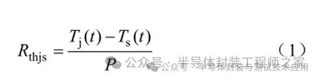
In the equation, Rthjs is the junction-to-heat sink thermal resistance; Tj(t) is the junction temperature; Ts(t) is the heat sink temperature; P is the power loss of the device.
1.3 Testing Platform and Process
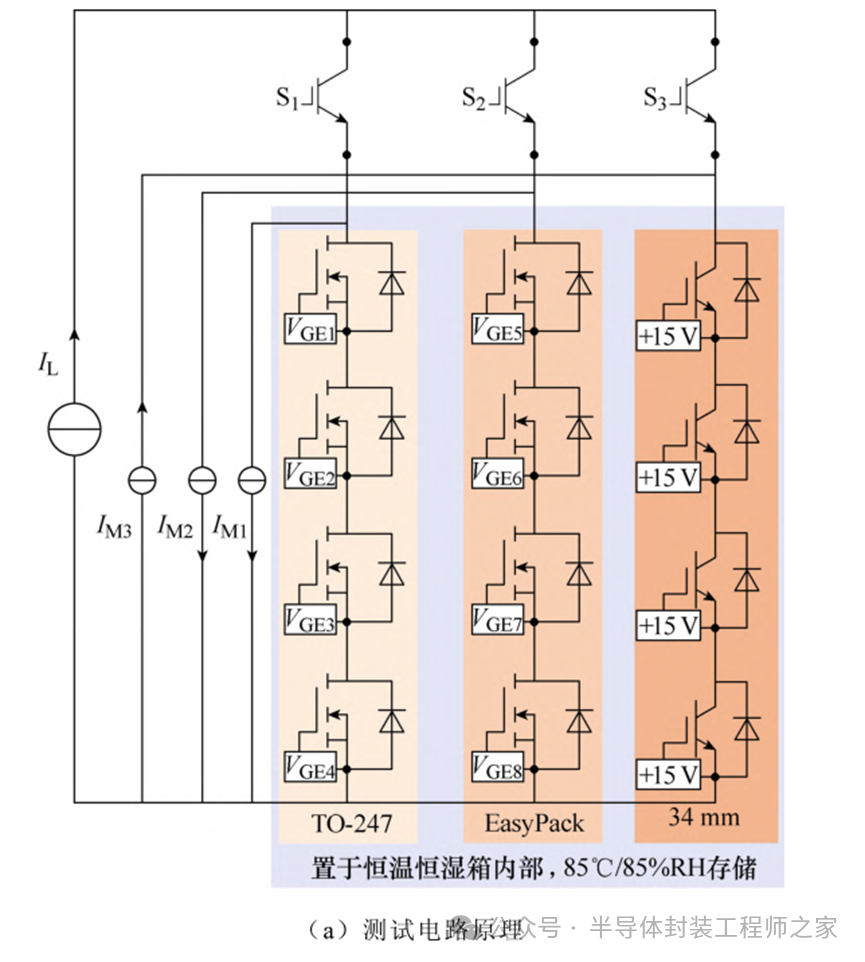
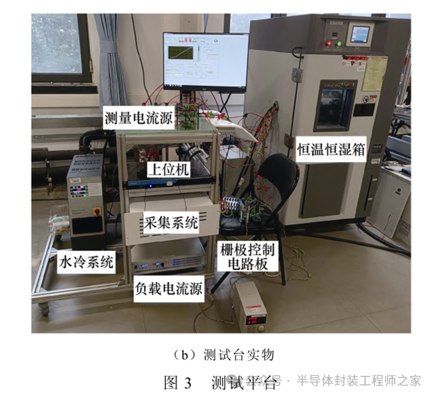
The testing circuit principle and physical setup are shown in Figure 3, where the DUTs and their connections, copper plates, heat sinks, etc., are placed in a constant temperature and humidity chamber, while the gate drive circuit board, current source, and water cooling unit are placed outside the chamber.
In Figure 3a, IL is the load current source used to heat the device; IM1, IM2, and IM3 are measurement current sources used to measure junction temperature; S1, S2, and S3 are current control switches that achieve switching between different branches, with each branch in series with four DUTs; the gate of the DUT is controlled by the drive signal. The testing principle of this platform has also been mentioned in other literature by our team [16-17]. In Figure 3b, the testing platform consists of a constant temperature and humidity chamber and a transient thermal impedance testing system, with relevant component information marked in the figure.
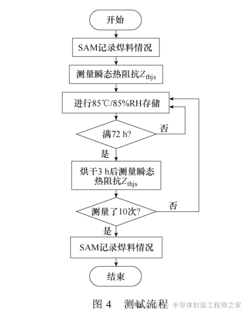
In terms of the testing process, first, a scanning acoustic microscope (SAM) is used to record the initial condition of the DUT solder, then the three groups of DUTs are placed in the constant temperature and humidity chamber for transient thermal impedance testing. To accelerate the moisture invasion rate without introducing new failure mechanisms, the constant temperature and humidity chamber is set to 85/85% °C RH to apply high temperature and high humidity stress. The relationship between the moisture diffusion coefficient D and temperature is given by

where D is the diffusion coefficient; D0 is the initial diffusion coefficient of the material; Ea is the activation energy; k is the Boltzmann constant; T is the temperature.
This temperature will not affect the aging of the device solder, surface corrosion, or changes in contact thermal resistance. Long-term storage at higher temperatures (e.g., 200 °C) will reduce shear and tensile stresses in the solder, thereby increasing the operational lifespan of the device [18]. The dual 85 storage is stopped every 72 hours to test the junction-to-heat sink transient thermal impedance Zthjs. After stopping, the devices need to be dried at 85 °C for 3 hours to ensure no moisture remains on the surface, avoiding any impact on the test results. It is worth noting that each time Zthjs is measured, care must be taken to avoid changing the wiring and moving the DUTs to eliminate interference from changes in contact resistance and reinstallation. Therefore, the entire device wiring and heat sink are placed inside the constant temperature and humidity chamber to achieve online monitoring of transient thermal impedance. During high temperature and high humidity storage, the water cooling system is turned off to avoid condensation, and when measuring Zthjs, the constant temperature and humidity chamber is turned off, and the water cooling system is turned on. Ultrasound scanning is performed at the beginning and end of the experiment, and the overall testing process is shown in Figure 4.
2 Testing Results and Analysis
2.1 Testing Results
After 722 hours of dual 85 storage, the results of 10 transient thermal impedance measurements are shown in Table 3. In Table 3, the horizontal line indicates that the adjacent two Zthjs measurement curves are completely consistent under dual 85 storage. If there is a change in adjacent Zthjs measurements, the change is presented in two parts: the proportion of change in steady-state thermal resistance (upper half of the cell) and the time constant interval corresponding to the change (lower half of the cell).
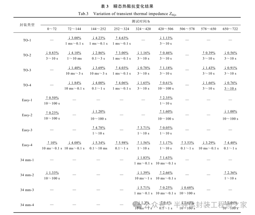
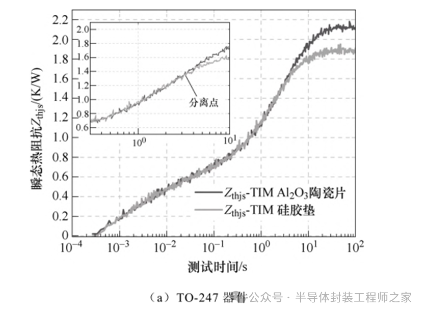
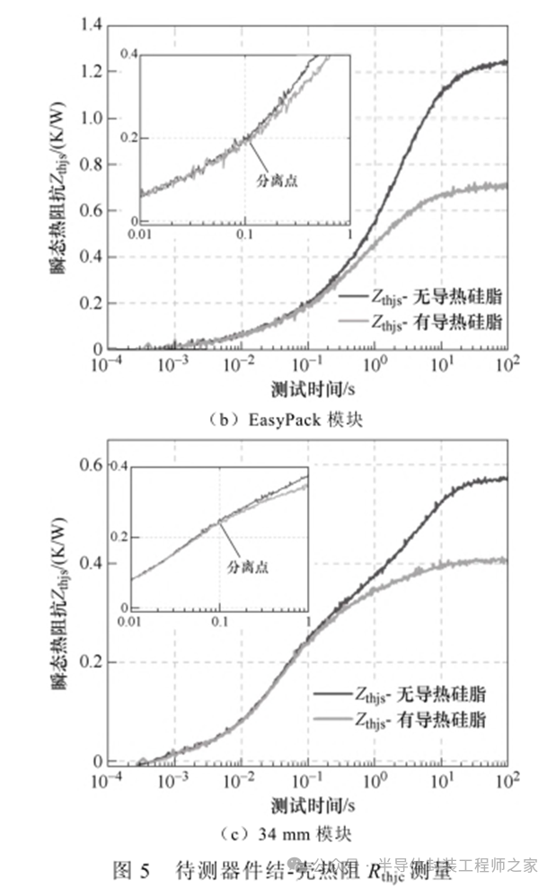
The results in Table 3 indicate that the impact of humidity on the thermal resistance of the device is divided into two parts: the change in chip solder thermal resistance (corresponding to a smaller time constant interval, such as 1 ms to 0.1 s) and the change in contact thermal resistance at the shell surface (corresponding to a larger time constant interval, such as 1 to 10 s). To accurately define the junction-to-case time constant of each DUT, the Transient Double Interface Method (TDIM) was used to measure the junction-to-heat sink transient thermal impedance of the DUTs, with results shown in Figure 5. The junction-to-case time constant of the TO-247 devices is 2.97 s, while the time constants for the EasyPack and 34 mm modules are 0.12 s and 0.10 s, respectively. To accurately determine the time constant corresponding to the separation point, the derivative of the thermal impedance was taken based on the transient double interface processing method, and the time constant corresponding to the separation point was determined to reduce the randomness in selecting the separation point. Based on the separation points of adjacent Zthjs tests and the corresponding junction-to-case time constants of the devices, it can be determined that moisture absorption occurs in the chip solder or shell surface.
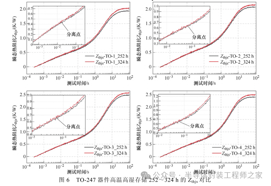
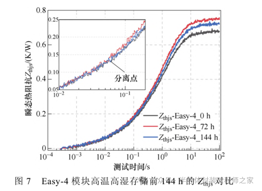
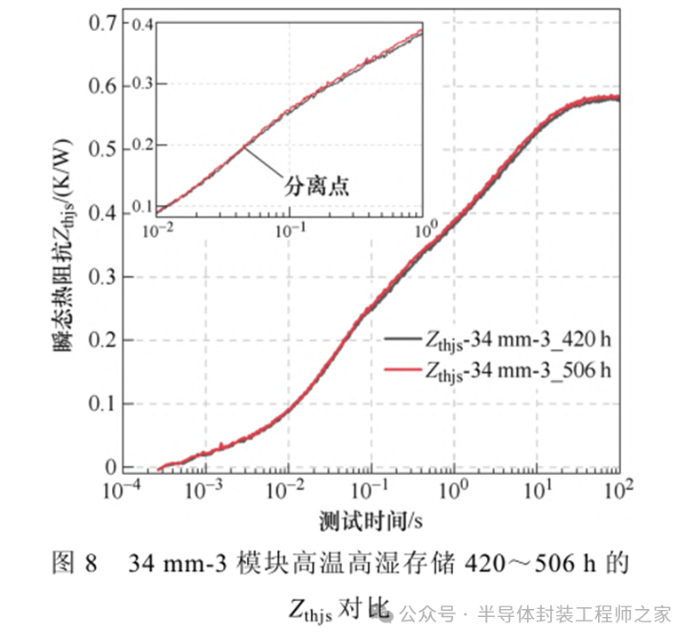
As shown in Table 3, all DUTs experienced changes in thermal resistance during the 722 hours of high temperature and high humidity storage test: for all DUTs in the TO-247 packaging, both chip solder thermal resistance and contact thermal resistance at the shell surface changed, with chip solder moisture absorption and copper substrate corrosion being the main reasons. Notably, all TO devices exhibited a regular phenomenon where the chip solder thermal resistance first decreased and then increased during the 72 to 324 hours period. The comparison of Zthjs for TO-247 devices during high temperature and high humidity storage from 252 to 324 hours is shown in Figure 6 and Table 3. This result further confirms that the chip solder of the device exhibits significant moisture absorption in high temperature and high humidity environments, thereby affecting the thermal resistance of the device. After 324 hours of high temperature and high humidity storage, the solder thermal resistance of all TO devices no longer changed, indicating that the moisture absorption of the chip solder had reached a stable state. For the EasyPack module, only device Easy-4 exhibited changes in chip solder thermal resistance, and its thermal resistance showed irregular changes from the beginning to the end of the experiment, which may be related to individual differences of this device. The Zthjs of device Easy-4 during high temperature and high humidity storage from 0 to 144 hours is shown in Figure 7. For the 34 mm module, devices 1 to 3 exhibited changes in chip solder thermal resistance during the 324 to 506 hours period, similar to the phenomenon observed in TO-247 devices during the 72 to 324 hours period, where the chip solder thermal resistance first decreased and then increased. Among them, the separation point of device 34 mm-3 is the most pronounced, with its transient thermal impedance curve Zthjs shown in Figure 8.
Furthermore, comparing the data in the table reveals that the TO-247 devices are affected by humidity earlier than the EasyPack or 34 mm modules (72 to 324 hours vs. 324 to 506 hours). However, in terms of material moisture absorption characteristics, epoxy resin has a lower moisture absorption capacity than silicone gel [19-20], which contradicts the phenomenon observed in this experiment. The reasons for this phenomenon are related to the size of the solder, the position of the solder, and the differences in parallel chips: in terms of solder size, the solder size of TO devices is only about 3.53 mm × 3.53 mm; in the EasyPack module, one bridge arm consists of four chips in parallel, with each chip’s solder size being about 4.19 mm × 3.23 mm, totaling 4.3 times the area of the TO device chip solder; the solder size of the 34 mm module is about 8.04 mm × 9.78 mm, which is 6.3 times the area of the TO device chip solder. In terms of solder position, the chip solder of TO devices and EasyPack modules is located at the center of the copper plate, while the chip solder of the 34 mm module is located at the edge of the copper plate. Among the parallel chips, only the EasyPack module consists of four chips in parallel, while the TO devices and 34 mm modules are single-chip devices.
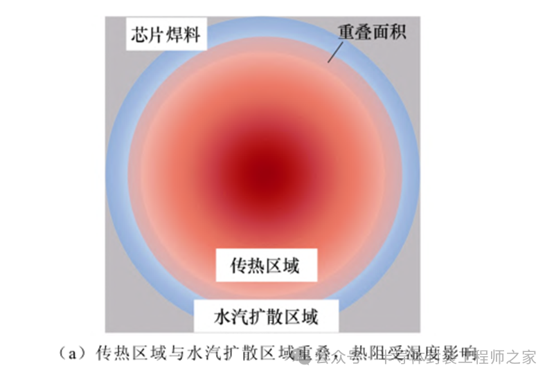
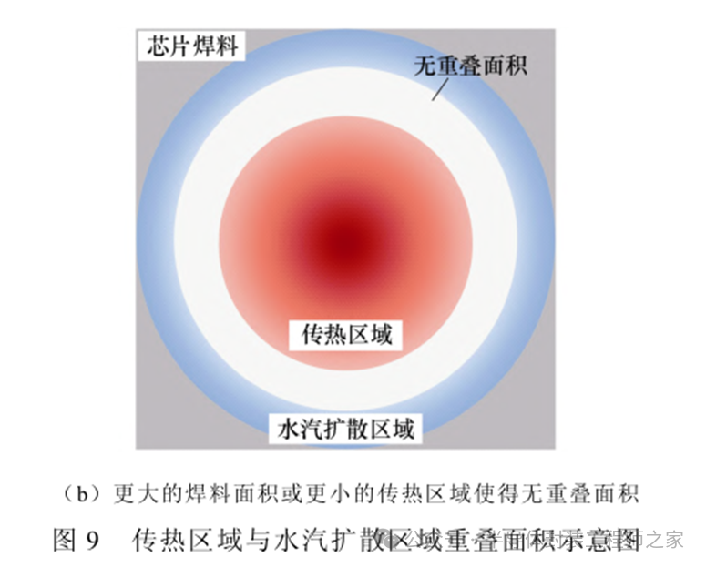
From Table 3, it can be seen that the time at which chip solder thermal resistance is affected by humidity is tTO-247 < t34 mm < tEasyPack. Comparing the test results of TO devices and 34 mm modules reveals that since water vapor diffusion occurs from the outside in, while heat transfer occurs from the inside out, the resistance encountered by the heat along its path is the thermal resistance. Therefore, the greater the overlap area between the water vapor diffusion area and the heat transfer area, the more susceptible the thermal resistance is to humidity. Under the same time and water vapor diffusion rate, a larger solder area means that the path for water vapor to diffuse to the center of the solder is longer, and the water vapor distribution at the edges has a weaker impact on the center solder (heat transfer area), causing the 34 mm module to be affected by humidity later, as shown in Figures 9a and 9b. If the water vapor diffusion area does not intersect with the heat transfer area during Zth testing, the thermal resistance remains unchanged. Comparing the test results of the 34 mm and EasyPack modules shows that the EasyPack chip solder area is small, yet the time it is affected by humidity tEasyPack is greater. This is because, on one hand, the EasyPack module consists of four chips in parallel, dividing the current flowing through a single chip by 1/4, resulting in Q=I2Rt, with the heat being only 1/16 of the original, significantly shortening the heat transfer area, as shown in Figure 9b. On the other hand, the position of the EasyPack module chip solder is closer to the center of the copper plate, which helps suppress the influence of humidity, as the diffusion coefficient of water vapor in copper is low, and the diffusion of water vapor through the copper plate to the chip solder is significantly inhibited.
2.2SAM Comparison and Visual Inspection
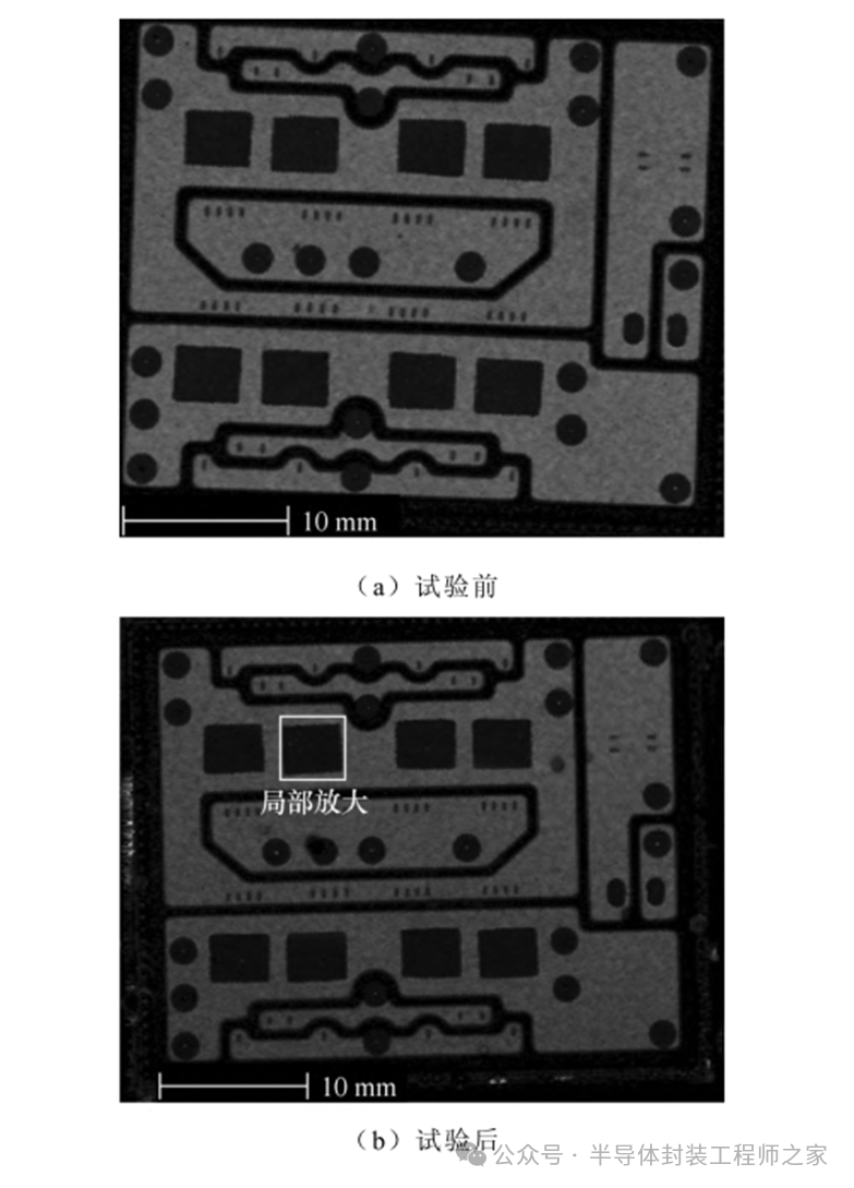
Before and after the tests, a SAM comparison was conducted on the DUTs, and almost all chip solders of the DUTs showed no significant aging signs, indicating that this process was not aging-related, nor were there any related voids. Some chip solders in the EasyPack module exhibited slight changes, appearing as dots, and the relevant SAM comparison is shown in Figure 10, where the changes in solder led to changes in thermal resistance.
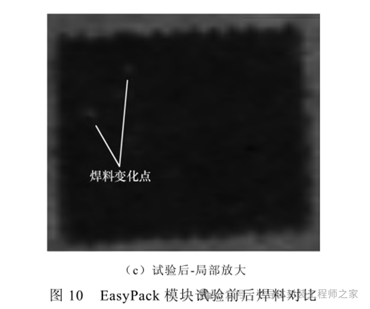
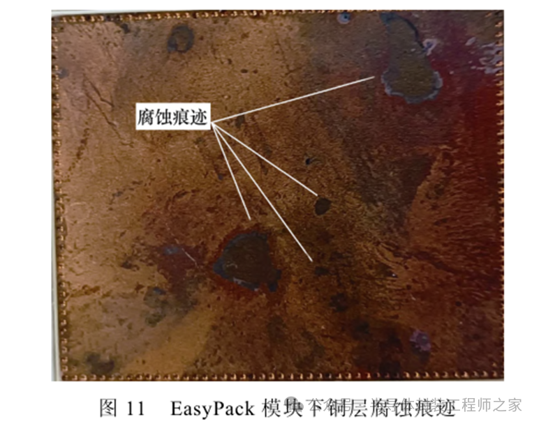
The corrosion traces on the copper layer under the EasyPack module are shown in Figure 11. In terms of visual inspection, Figure 11 shows that the bottom copper plates of modules Easy-1 to Easy-4 and devices TO-1 to TO-4 have been corroded to varying degrees, with the phenomenon being more pronounced in the EasyPack module. This phenomenon is the fundamental reason for the change in contact thermal resistance at the device shell surface.
3 Investigation of the Mechanism of Change in Chip Solder Thermal Resistance
Considering that the test results of the TO-247 devices in Table 3 are relatively consistent, and the modeling of TO devices is relatively simple, modeling and simulating them can better reflect the basic laws of humidity’s effect on thermal resistance. Therefore, this section establishes a simulation model for the IMW65R048M1H DUT to explore the mechanism of thermal resistance change under high temperature and high humidity storage.
3.1 Simulation Model and Thermal Characteristic Calibration
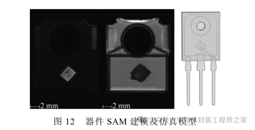
The lateral dimensions of the IMW65R048M1H device were obtained through SAM, while the longitudinal dimensions were obtained based on literature [21-23] and relevant design experience. The SAM modeling and simulation model of the device are shown in Figure 12.
To more accurately describe the mechanism by which humidity affects the thermal characteristics of the device, and to compare with experimental phenomena, the thermal characteristics of the device must first be calibrated based on transient thermal impedance Zthjs testing data. In the calibration model, the DUT is fixed to the copper plate using an alumina ceramic sheet, which is fixed to the surface of the heat sink. The relevant boundary conditions are set as shown in Figure 13.
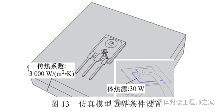
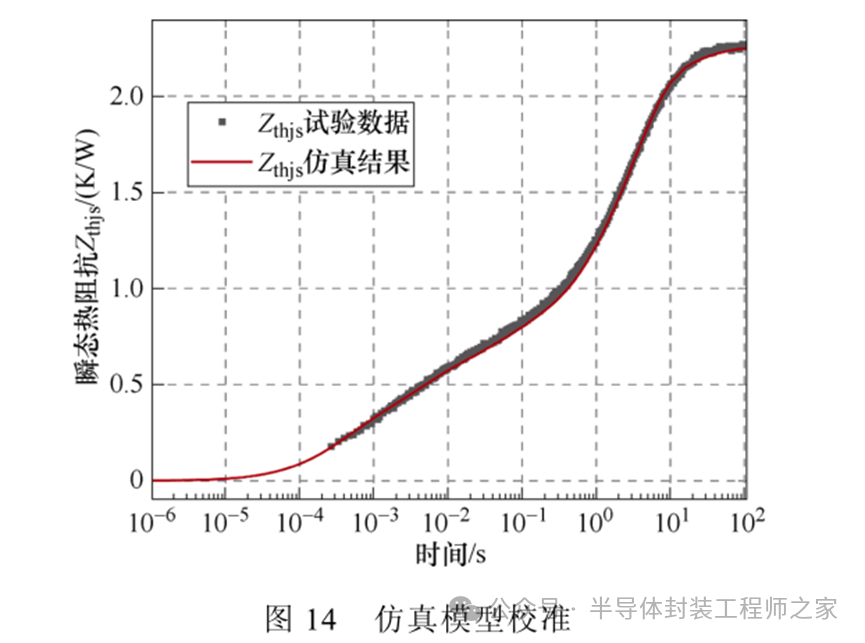
In the transient thermal impedance simulation, the heating time ton, cooling time toff, and load current IL settings are consistent with the experiments, as shown in Table 2. The calibration results are shown in Figure 14, where the simulation results align well with the experimental data, indicating that the thermal path of the simulation model is generally consistent with the actual conditions.
3.2 The Mechanism of Humidity’s Impact on Thermal Characteristics
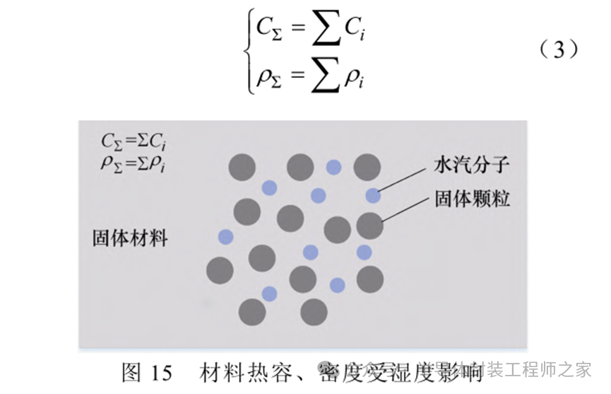
At the microscopic level, water vapor diffuses into the device packaging from the environment in the form of water molecules. If we do not consider the chemical reactions between the water molecules and the material molecules, the microscopic physical manifestation is that water molecules embed themselves in the gaps of the existing material molecules. After moisture invasion, at the macroscopic level, the physical properties of the material change, and the thermal characteristics of the material (thermal capacity, density, thermal conductivity) also change accordingly [24-25]. For the entire material, the total thermal capacity CΣ and total density ρΣ should be the summation of the thermal capacity Ci and density ρi of the material at each point in space, and the arrival of water molecules increases this summation result, as shown in Figure 15.
For the total thermal conductivity λΣ of the material, the situation is slightly more complex. The total thermal conductivity λΣ within the material should be the parallel summation of the thermal conductivity λi along each heat transfer path, as shown in Equation (4) and Figure 16.
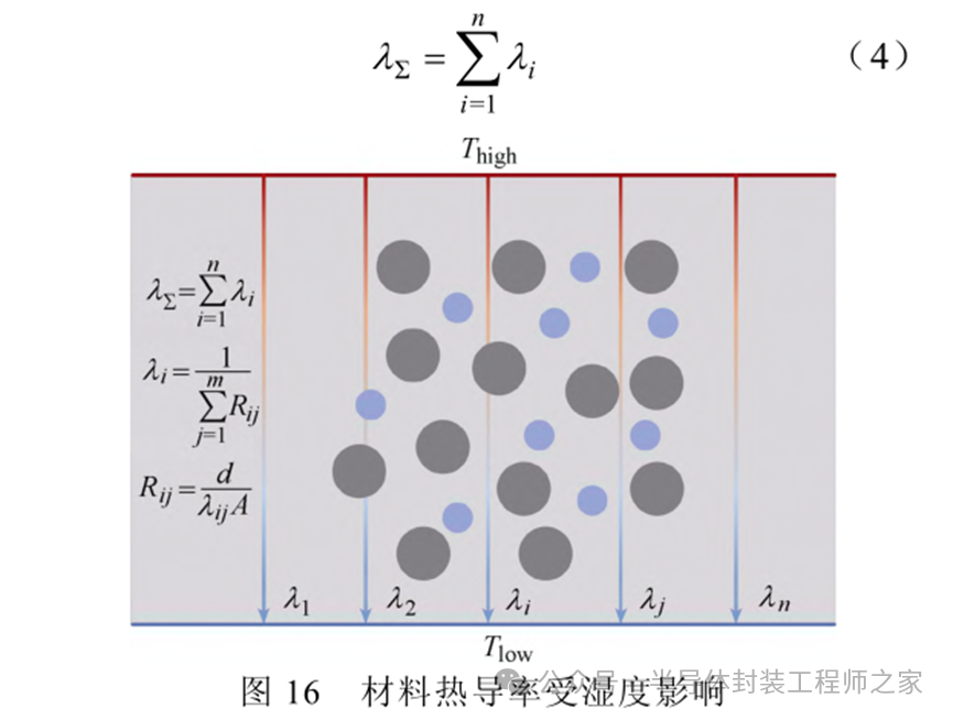
For each heat transfer path λi, it is obtained by summing the micro-element thermal resistances Rij along that path and taking the reciprocal. Rij can be calculated based on the definition formula, as shown in
where d is the micro-element thickness; λij is the thermal conductivity at the micro-element; A is the micro-element area. The invasion of water vapor leads to changes in the micro-element thermal resistance Rij, which in turn changes the thermal conductivity λi of the heat transfer path where that micro-element is located, and after parallel summation, the total thermal conductivity λΣ changes.
As shown in Figures 15 and 16, the invasion of humidity leads to changes in material thermal capacity, density, and thermal conductivity. Since TO-247 devices are mainly composed of epoxy resin, chip passivation layers, and chip solder that absorb moisture, and the chip solder directly affects packaging reliability and operational lifespan, the analysis focuses on the impact of moisture invasion on the thermal resistance of chip solder. Table 4 compares the thermal characteristics of water vapor and chip solder, revealing that the thermal conductivity ratio of water vapor to chip solder is only 1:93.2, while the constant pressure thermal capacity ratio is 19.2:1. The significant differences in material thermal characteristics will further reflect on the thermal characteristics of the device.
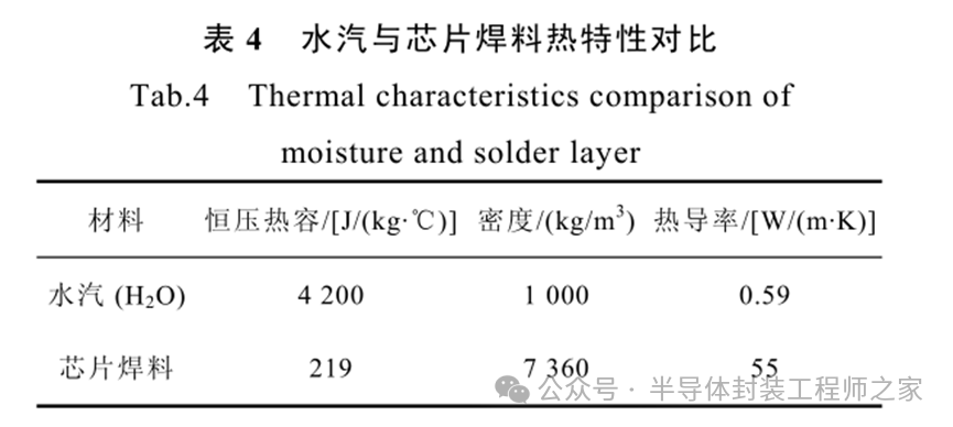
Furthermore, to quantify the impact of humidity on the thermal capacity, density, and thermal conductivity of chip solder, a case analysis is conducted: due to moisture invasion, the weight gain of the device is on the order of 0.1% [26]. Assuming that the water vapor content accounts for only 0.1% of the total material in the chip solder layer, filling the gaps in the original material molecules, and that water molecules and solid material molecules are uniformly distributed, the changes in thermal capacity, density, and thermal conductivity of the material are evaluated. From Equation (3), it is calculated that CΣ = 1 × 219 + 0.1% × 4200 = 223.2 J/(kg·℃), ρΣ = 1 × 7360 + 0.1% × 1000 = 7361 kg/m3. The thermal capacity CΣ and density ρΣ of chip solder change by 1.9% and 0.0135%, respectively, compared to when there is no moisture invasion. For the calculation of thermal conductivity, from Equation (5) and Table 4, it can be seen that the micro-element thermal resistance of water vapor is 93.2 times that of the chip solder micro-element (Rij@H2O=93.2Rij@Solder). Let m be the total amount of chip solder in each heat transfer path, and n be the number of heat transfer paths. Assuming that water vapor is uniformly distributed, after moisture invasion, each heat transfer path λi′ consists of 0.1% water vapor and 100% chip solder, thus λi′ = 1/(1‰mRij@H2O+mRij@Solder) = 1/(1.0932mRij@Solder). For the original heat transfer path (when water vapor has not invaded), λi = 1/(mRij@Solder), thus λi′ = (1/1.0932) λi. Furthermore, when water vapor has not invaded, the total thermal conductivity λΣ of chip solder is calculated from Equations (3) and (6) as follows:

After moisture invasion, the total thermal conductivity λ′Σ of chip solder is calculated from Equations (3) and (7) as follows: after moisture invasion, the total thermal conductivity λ′Σ = 0.914 λΣ.
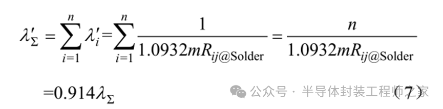
From the theoretical derivation above, it can be seen that moisture invasion on the order of 0.1% can significantly cause changes in the thermal characteristics of chip solder, specifically an increase in thermal capacity and density by 1.9% and 0.0135%, respectively, and a decrease in thermal conductivity by 8.6%. Of course, this result is strongly correlated with the amount of moisture absorbed, and under appropriate simplifications, the actual situation is more complex. To further explore the impact of solder thermal characteristic parameters on transient thermal impedance, different thermal capacities and thermal conductivities are set for the chip solder of the IMW65R048M1H device (the impact of density changes on thermal resistance can be neglected) to investigate their effects on the junction-to-heat sink transient thermal impedance Zthjs, as shown in Figure 17. The results indicate that increasing the thermal capacity of the solder layer leads to a decrease in the thermal resistance of the solder layer only (corresponding time constant 30 μs to 45 ms), while the overall thermal resistance remains unchanged; decreasing the thermal conductivity of the solder layer leads to an increase in the overall thermal resistance of the device (corresponding time constant 150 μs and beyond). This pattern also applies to higher moisture absorption rates (thermal capacity of chip solder increases by 50% or more, thermal conductivity decreases by 20% or less).
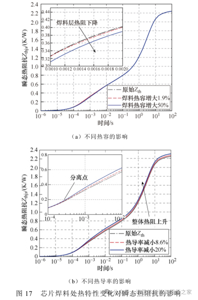
Furthermore, as seen in Figure 6, the transient thermal impedance of TO-247 devices exhibited separation during the 252 to 324 hours period (the separation point corresponds to a time constant of 1 ms to 0.1 s), and the thermal resistance of all devices increased. This phenomenon can be explained by Figures 15 to 17: as shown in Figures 15 and 16, the invasion of humidity increased the thermal capacity of chip solder and decreased its thermal conductivity; as shown in Figure 17, the increase in thermal capacity leads to a decrease in the thermal resistance of the solder layer (with overall thermal resistance unchanged), while the decrease in thermal conductivity leads to an increase in the overall thermal resistance of the device and the presence of a separation point (the separation point corresponds to a time constant of 0.15 to 10 ms, during which thermal conductivity plays a dominant role). Therefore, it can be concluded that the invasion of water vapor into chip solder increases thermal capacity and decreases thermal conductivity, resulting in an increase in overall device thermal resistance and the emergence of a separation point. This conclusion is corroborated by the experimental results in Figure 6.
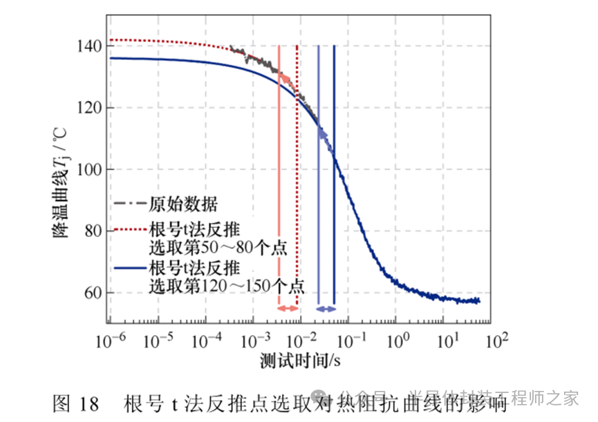
Additionally, the time constant of the separation point in the simulation cannot be completely matched with the time constant measured in the experiments due to several factors: the selection of the maximum junction temperature Tjmax measurement delay time tMD in the experiment, the selection of points for the square root t method, the sampling frequency and noise of the equipment, and the differences in thickness and thermal conductivity of the actual chip or chip solder. As noted in Section 1.2, tMD=200 μs > 0.15 ms, leading to deviations in the measurement of the initial thermal resistance value. Furthermore, differences in the selection of points for the square root t method also cause the measurement curves to drift, resulting in changes in the separation points of adjacent thermal resistance curves, as shown in Figure 18.
Similarly, the separation of thermal resistance curves in Figures 7 and 8 is also determined by the increase in thermal capacity and decrease in thermal conductivity of chip solder, with thermal conductivity being the dominant factor. Additionally, the phenomenon where the chip solder thermal resistance of TO devices and 34 mm modules first decreases and then increases during the moisture absorption process, as shown in Table 3, may be due to the initial invasion of water vapor filling the gaps at the material interface, resulting in better interface smoothness and a decrease in contact thermal resistance. As moisture continues to invade, the thermal performance of the chip solder gradually declines, leading to an increase in thermal resistance. This phenomenon can be further verified through molecular dynamics simulations, which will not be elaborated on here.
In summary, water vapor invades the chip solder from the outside in, initially filling the gaps at the material interface, which causes a decrease in both chip solder and overall device thermal resistance. Once the interface is saturated, moisture continues to diffuse into the chip solder, leading to an increase in thermal capacity and a decrease in thermal conductivity within the chip solder, corresponding to a decrease in chip solder thermal resistance (with overall thermal resistance unchanged) and an increase in overall device thermal resistance. During this process, the decrease in thermal conductivity plays a dominant role, resulting in an increase in device thermal resistance and the emergence of a separation point.
4 Conclusion
This paper investigates the mechanism by which humidity affects the thermal resistance of chip solder in power devices of different packaging types. An experimental platform integrating transient thermal impedance testing and constant temperature and humidity chamber equipment was established. Based on the testing process, the phenomenon of humidity’s impact on chip solder thermal resistance was confirmed, and the mechanism by which humidity affects chip solder thermal resistance was proposed for the first time. Through case studies and simulation models, the following conclusions were drawn:
1) In high temperature and high humidity environments, humidity diffuses from the environment into the device, leading to changes in the junction-to-heat sink transient thermal impedance Zthjs of the device. All TO-247 devices and 34 mm module chip solder thermal resistances changed, while only the chip solder thermal resistance of device 4 in the EasyPack module changed.
2) The impact of humidity on the junction-to-heat sink thermal resistance of the device comes from two aspects: ① the impact on the internal chip solder thermal resistance of the device, leading to an increase in material thermal capacity and density and a decrease in thermal conductivity, thereby affecting the junction-to-heat sink thermal resistance; ② the impact on the contact thermal resistance at the shell surface of the device, which corrodes the copper substrate of the device, thereby affecting the junction-to-heat sink thermal resistance.
3) Combining case studies and the calibrated finite element simulation model of thermal characteristics, the results indicate that when the water vapor content accounts for 0.1% of the chip solder, the thermal capacity, density, and thermal conductivity of the chip solder change to 101.9%, 100.0135%, and 91.4% of their original values, respectively. The fundamental reason is the significant differences in material thermal characteristic parameters. The increase in thermal capacity of the solder layer leads to a decrease in the thermal resistance of the solder layer (with overall thermal resistance unchanged), while the decrease in thermal conductivity of the solder layer leads to an increase in the overall junction-to-heat sink thermal resistance of the device, where the decrease in thermal conductivity plays a dominant role, resulting in an increase in device thermal resistance and the emergence of a separation point.

Disclaimer: This article is original or forwarded by the author. If it inadvertently infringes on someone’s intellectual property, please inform us for deletion.If there are any infringements, please contact us in a timely manner, and we will delete it within 24 hours.The content of the article represents the author’s personal views, and the semiconductor packaging and testing technology application only reprints it to convey a different viewpoint, which does not represent the endorsement or support of the semiconductor packaging and testing technology application for this viewpoint. If there are any objections, please feel free to contact the semiconductor packaging and testing technology application..