Despite many companies in the semiconductor industry focusing on developing AI chips for nearly 12,000 data centers worldwide, the chips powering over 20 billion IoT devices globally are also undergoing significant innovations.
Prediction 1
Edge AI Integrated into IoT Chips to Accelerate Development
Integrating edge artificial intelligence into IoT devices will initiate a significant shift towards hardware with AI capabilities.
Currently, most IoT devices lack the built-in computing power required to run AI workloads. Although the demand for local inference is growing to improve latency, resilience, bandwidth efficiency, and privacy, the majority of the 21 billion IoT endpoints deployed today still rely on external processing or simple rule-based logic. This gap between demand and capability lays the groundwork for transformation in 2026.
NPU and AI-enabled cores are entering mainstream IoT design. Manufacturers are extending edge AI across all levels of IoT. In recent years, only a small fraction of IoT products (typically industrial gateways, advanced cameras, and high-end modules) have integrated neural processing units (NPUs) or low-power AI accelerators. Now, manufacturers are beginning to promote these capabilities to a broader range of device categories. New IoT system-on-chip (SoC) designs incorporate lightweight NPUs, vector extensions, and AI cores similar to digital signal processors (DSPs) to support tasks such as anomaly detection, small model vision, local audio intelligence, and status monitoring, which can be performed directly on the device.
IoT Analytics predicts that 2026 will see the first wave of IoT devices equipped with edge AI acceleration technology. By then, shipments of AI-enabled chipsets will expand into areas such as sensors, IoT connectivity modules, industrial PCs, and mid-range gateways, which previously lacked any device-side AI inference capabilities.
More complex SoC designs drive demand for AI-ready tools. AI features are influencing the design priorities of IoT chips. Embedding NPUs and AI modules into IoT chips increases design complexity, particularly concerning thermal budgets, validation, memory bandwidth, and security. Consequently, IoT chip suppliers are increasingly relying on electronic design automation (EDA) tools optimized for AI computational analysis, reusable intellectual property (IP) such as low-power NPUs and secure enclaves, and mature processes optimized for mixed workloads (compute + connectivity + security). These demands are emerging across various sectors, including consumer, industrial, automotive, and energy IoT.
IoT Analytics expects that by 2026, AI-aware EDA processes and ready-made AI IP subsystems will be more widely adopted in IoT chip development. These tools and IP modules will reduce design complexity and lower the barrier to adding small model inference capabilities to mass-market IoT devices.
Edge AI is becoming a key differentiator for IoT OEMs. Device manufacturers are linking AI with functional innovation. As hardware with AI capabilities becomes more prevalent, device manufacturers are beginning to view local inference as a competitive advantage, enabling features such as privacy-preserving analytics in smart home devices, real-time defect detection in industrial sensors, or offline wake word detection in consumer electronics.
IoT Analytics predicts that 2026 will be a turning point for IoT OEMs, transitioning from pilot phases in early 2025 to large-scale product portfolio updates, marketing these products as edge AI-enabled IoT devices. This shift will accelerate the transition from basic telemetry devices to endpoint devices that support local inference for device-side decision-making.
Prediction 2
Chipset and RISC-V-based IoT Chip Shares Will Increase
Modular and RISC-V are becoming increasingly popular in the IoT space. Over the past two years, rising cost pressures, higher integration requirements, and the need for more flexible architectures have influenced the design of IoT semiconductors. These trends have prompted suppliers to shift towards modular design approaches (such as chiplets) and open instruction set architectures (ISAs) like RISC-V. As these trends continue, the groundwork laid indicates that by 2026, IoT chips based on chipsets and RISC-V will see significant growth.
Chiplets are replacing single-chip system-on-chip (SoC) in new designs. Industry dynamics from 2024-2025 indicate a clear shift from single-chip SoCs to partitioned modular designs. Chiplet architectures separate computing, storage, and I/O functions into smaller chips that can be produced on different process nodes and connected via high-bandwidth interfaces. This reduces mask costs, improves yields, and allows targeted upgrades without redesigning the entire SoC. Recent examples include the Eagle-N, a chiplet-based AI accelerator for automotive systems launched by Tenstorrent and BOS Semiconductors; and Intel’s announcement of a multi-node, chiplet-based SoC for software-defined vehicles.
IoT Analytics expects that by 2026, the application of chiplets in IoT, automotive, and AI chipsets will grow significantly. Companies will transition from early custom chiplet designs to more widespread use of standardized computing, connectivity, and security chiplets. This modular approach will reduce engineering workloads, shorten development cycles, and lower non-recurring engineering costs for AI, automotive, and IoT SoCs.
RISC-V is enabling customized low-power IoT chips. As manufacturers seek flexibility, lower licensing costs, and the ability to customize CPUs for specific devices, RISC-V is rapidly advancing in the IoT space. Its open modular instruction set architecture (ISA) allows companies to build differentiated processors without relying on a closed IP ecosystem. This drives rapid experimentation and commercial deployment in areas such as wearables, microcontrollers, and low-power edge devices.
IoT Analytics expects that the RISC-V architecture will further expand into low-power IoT edge devices, edge AI processors, and automotive subsystems by 2026. Growth will be strongest in markets prioritizing supply chain autonomy and deeper architectural control to customize CPU cores for specific edge and automotive workloads.
Prediction 3
More IoT Chip Designs Will Consider Carbon Emissions
The application of RISC-V architecture in the IoT space is rapidly growing. With regulations such as the EU Corporate Sustainability Reporting Directive (CSRD) and increasing customer expectations, sustainability requirements are becoming increasingly specific for semiconductor suppliers, and carbon emissions transparency is becoming essential. Carbon emissions tracking is increasingly viewed as a core constraint in IoT design, now discussed alongside power consumption, performance, area, and cost (PPAC), rather than as a standalone reporting item.
Carbon emission metrics have become part of the semiconductor design workflow. Developments in 2024-2025 indicate that carbon emission data is beginning to be integrated into daily engineering workflows. Some EDA suppliers have incorporated emission data into early architectural trade-off analyses. For example, in May 2025, U.S.-based EDA, hardware, and IP supplier Cadence joined the Sustainable Semiconductor Technologies and Systems (SSTS) project at imec in Belgium, aiming to integrate process and supply chain emission data directly into the design environment, allowing engineers to compare carbon emission impacts just as they would compare power, performance, and area (PPA) metrics. IP suppliers are also expanding their deliverables to include sustainability metadata and lifecycle assumptions, enabling integrators to pass carbon emission estimates to system-level simulations and procurement stages.
IoT Analytics predicts that by 2026, carbon emission metrics will be more widely integrated into the IoT semiconductor design workflow. EDA and IP suppliers will incorporate emission data into early assessments for PPAC, allowing engineers to consider carbon emission impacts in regular architectural trade-offs.
IoT Chip Manufacturers Are Improving Carbon Emission Reporting Standards. Foundries and chip suppliers are generally enhancing the granularity of sustainability reporting, making it easier for original equipment manufacturers (OEMs) to incorporate carbon emission impacts into component selection. IoT Analytics predicts that by the end of 2030, connected IoT devices will reach 39 billion units, making accurate collection of sustainability reporting details crucial for the entire IoT ecosystem, and IoT semiconductor companies are beginning to take action.
In June 2024, Germany-based semiconductor design and manufacturing company Infineon expanded the carbon footprint disclosure of its MCUs and connectivity devices to cover materials, manufacturing, and logistics, allowing OEMs to focus not only on operational energy efficiency but also on their embedded carbon emissions when evaluating products. In April 2025, Taiwan-based chip foundry TSMC committed to joining the Science Based Targets initiative (SBTi) and providing node-level carbon footprint data while actively encouraging its suppliers to adopt renewable energy.
IoT Analytics expects that 2026 will accelerate the transition of major wafer foundries and IoT chip suppliers towards standardized, auditable carbon emission disclosures. Chiplet companies will shift from decentralized sustainability reporting to structured product-level and node-level information disclosures, which will be directly imported into OEM procurement tools. This will enable procurement teams to compare embedded carbon emissions with pricing, performance, and qualification data, making the selection of carbon emission-sensitive components a routine aspect of IoT design.
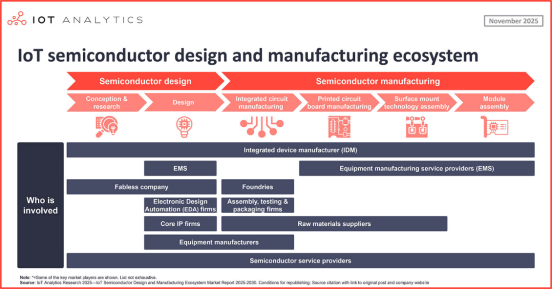
As shown in the image above, semiconductor design and manufacturing encompass six major stages from concept and research to module assembly. IoT Analytics categorizes these stages into ten types of stakeholders. IoT chips follow the same value chain steps as other semiconductor chips. The “2025-2030 IoT Semiconductor Design and Manufacturing Ecosystem Market Report” focuses on the three stages where IoT chips are actually specified and produced: IoT EDA, IoT SIP, and IoT foundries.
IoT EDA. Companies providing software tools to design chips and modules for IoT endpoints and gateways. This includes register transfer level (RTL), simulation, validation, synthesis, design for testability (DFT), packaging, and printed circuit board (PCB) tools used for IoT microcontroller units (MCUs), connectivity integrated circuits (ICs), sensors, and system-on-chips (SoCs).
Software IP for IoT. Refers to companies that license reusable intellectual property (IP) modules for IoT chips; for example, CPU and MCU cores, NPUs, security elements, and interconnect IP. Revenue is derived solely from IP used in IoT endpoint or gateway SKUs.
IoT Wafer Foundries. Companies manufacturing wafers and advanced packaging for IoT endpoint and gateway chips. This includes mature and advanced process nodes, embedded non-volatile memory, RF and analog processes, as well as system-in-package (SiP) or 3D IC packaging for IoT modules.
Prediction 4
More IoT Devices Will Be Produced Locally
Countries are investing in local semiconductor manufacturing along the IoT value chain. As part of a broader strategy to secure technology supply chains and reduce geopolitical risks, governments are intensifying efforts to promote local semiconductor production. By 2026, the manufacturing, packaging, and assembly of IoT chips will increasingly occur within regional ecosystems rather than being concentrated in a single area.
Governments are tightening control over semiconductor supplies, including IoT chips. Initially, semiconductor policies in various countries focused on cutting-edge logic chips, but recent initiatives indicate that governments are expanding their regulatory scope to include key components of IoT devices such as microcontrollers, connectivity chipsets, security elements, and sensor-grade silicon chips. These initiatives suggest that IoT silicon chips are no longer viewed purely as commodities but as critical components of national digital infrastructure.
IoT Analytics expects that by 2026, more regulatory measures targeting IoT-grade semiconductors will be introduced. Countries are investing in the development of domestic IoT chip production. In recent years, many countries have launched large-scale industrial programs to fund domestic manufacturing capability building.
United States—The CHIPS and Science Act allocates $52.7 billion to promote domestic manufacturing and R&D. Additionally, the government has expanded funding for semiconductor production companies such as Intel, TSMC, and Samsung.
China—China promotes domestic chip manufacturing through the Big Fund policy and aims to close the technology gap by 2030.
Japan—The Japanese government has committed to invest approximately $65 billion by 2030 to expand its semiconductor and AI industries, supporting domestic wafer fabs and R&D collaborations.
South Korea—Korean officials announced a $19 billion support plan to strengthen its chip supply chain and the competitiveness of small and medium-sized enterprises in 2024.
European Union—The EU is guiding investments under the EU Chips Act to achieve localization of production, secure raw material supplies, and establish technological sovereignty among member states.
IoT Analytics expects that by 2026, many new and expanded domestic and regional wafer fabs focusing on IoT-related semiconductor processes (such as mature node logic, analog, embedded non-volatile memory, and RF) will begin to produce or gradually achieve commercially viable mass production. As these capacities come online in the coming years, chiplet suppliers and countries will be better positioned to build a more autonomous regional core IoT component supply chain.
Prediction 5
IoT Chip Design Will Rely Heavily on AI
AI is becoming a core component of the IoT chip design workflow. Over the past two years, EDA suppliers have been working to integrate AI into both front-end and back-end design processes, providing semiconductor teams with new methods to automate labor-intensive tasks, validate constraints, and identify issues earlier. These capabilities are particularly important for IoT chips, which face strict limitations in power consumption, area, and cost, leaving little room for design iterations.
AI is gradually permeating all aspects of the semiconductor design process. Developments from 2024 to 2025 indicate that AI is beginning to assist the entire design process rather than being limited to isolated tools. In July 2025, U.S.-based Siemens Digital Industries Software released a suite of AI-enhanced tools covering the entire process from schematic capture to physical implementation, including features such as validation automation, constraint analysis, and early defect detection. These tools are designed to support semiconductor and PCB design, which is crucial for integrating RF, sensor, and computing functions into the constrained sizes of IoT vendors.
IoT Analytics expects that by 2026, AI-assisted validation, constraint checking, and layout optimization technologies will be more widely adopted, especially among IoT design teams building edge AI chipsets, connected SoCs, and mixed-signal devices. As these AI-driven EDA workflows mature, they will help teams shorten iteration cycles, reduce implementation errors, and address the increasing complexity of integrating RF, sensor, and computing in compact IoT devices.
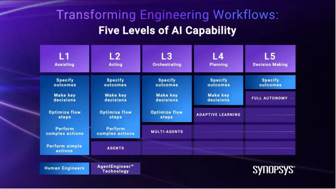
EDA companies are planning the path to autonomous design agents. Vendors are also developing roadmaps for AI systems whose capabilities extend beyond generating code or suggesting optimizations. For example, the CEO of U.S.-based EDA software company Synopsys, Sassine Ghazi, outlined a roadmap in March 2025 where current generative AI design tools will evolve into fully autonomous multi-agent design systems. These “agent engineers” are expected to support IP integration, advanced packaging, process node selection, and lifecycle management, all of which directly impact IoT chips, as IoT chips increasingly integrate digital logic, RF, power management, and sensing functions into a single package.
IoT Analytics expects that early forms of intelligent AI will enter the IoT chip development workflow by 2026, primarily as workflow assistants coordinating existing EDA tools to perform tasks such as validation, IP integration, and physical design exploration. These systems will be able to automate routine steps, propose constraints and layout schemes, and manage multi-tool design processes, while engineers still retain control over architectural choices, final approval decisions, and safety-critical validations.
Prediction 6
IoT Security Design Will Become an Indispensable Element
IoT security design is becoming a mandatory requirement in the global market. Security design has shifted from best practice to regulatory expectation, and this shift has particularly significant implications for IoT. IoT devices operate in widely distributed and resource-constrained environments (such as factories, homes, vehicles, and energy systems) and cannot rely on traditional boundary security protections. Their longer lifecycles, remote deployments, and continuous connectivity make hardware-level protection crucial for security, reliability, and compliance. These realities are prompting suppliers to integrate more robust chip-level security features into the IoT value chain.
Compliance requirements are driving the evolution of IoT security architectures. Regulatory frameworks such as the EU Cyber Resilience Act, the U.S. National Institute of Standards and Technology (NIST) post-quantum roadmap, and the United Nations Economic Commission for Europe (UNECE) R.155 and R.156 increasingly require devices to have verifiable hardware protection measures before sale. For IoT suppliers, this means that features such as hardware roots of trust, secure boot, and physical unclonable function (PUF)-based authentication are no longer optional but prerequisites for certification in industries such as industrial automation, automotive, healthcare, and smart homes.
IoT Analytics expects that by 2026, high-end IoT microcontrollers (MCUs), connectivity chipsets, security elements, and edge AI processors will more widely adopt hardware-enforced security baselines. As regulatory requirements tighten, hardware roots of trust, secure boot, and tamper-proof identities will become standard entry conditions for the high-end IoT market. In contrast, low-cost IoT devices will continue to focus security measures on lighter software layers, such as secure boot and secure operating system support, rather than relying entirely on hardware security guarantees.
Vendors are building tools to ensure long-term compliance for IoT devices. As compliance requirements become stricter, vendors are redesigning chip architectures and investing in compliance tools to help IoT device manufacturers meet lifecycle compliance obligations. For example, U.K.-based IoT cybersecurity company Crypto Quantique is automating secure configuration, certificate lifecycle management, and vulnerability tracking, which are crucial for IoT original equipment manufacturers (OEMs) since devices may need to be deployed for 10 to 20 years without physical access. Meanwhile, U.S.-based semiconductor design and manufacturing company Qualcomm is standardizing secure boot processes, generating signed software bill of materials (SBOM), and integrating monitoring mechanisms to help suppliers maintain long-term compliance across deployed device fleets.
IoT Analytics expects that by 2026, an end-to-end compliance ecosystem supporting secure configuration, certificate management, software bill of materials maintenance, and vulnerability monitoring throughout the device lifecycle will be more widely adopted. Regulated industrial, medical, and automotive IoT OEMs are increasingly combining internal security capabilities with external compliance-as-a-service platforms to meet long-term regulatory obligations without having to build all tools in-house.
Post-quantum cryptography is moving into the IoT hardware space. The rise of quantum computing has heightened the urgency of post-quantum cryptography, especially for IoT devices that will operate for decades and are difficult to replace. The guidance from the U.S. National Institute of Standards and Technology (NIST) on transitioning to post-quantum cryptography (PQC) by 2035 is prompting semiconductor suppliers to embed quantum-safe algorithms (such as module lattice-based key encapsulation mechanisms (ML-KEM)) into hardware. Infineon’s EAL6 certified PQC hardware (TEGRION security controller) exemplifies the rapid transition of these capabilities from roadmap concepts to commercial products.
IoT Analytics expects that, driven by the demand for long lifecycles in sectors such as energy infrastructure, industrial automation, automotive gateways, and connected medical devices, 2026 will see the first pilot implementations of PQC-supporting security modules in high-value IoT chips. Currently, PQC applications are still limited to high-end devices, but as suppliers begin preparing for NIST’s 2035 migration timeline, PQC is expected to become an important design consideration.
Source: Semiconductor Industry Insights